[SSE3021 Digital Integrated Circuit Design] Schematic and Layout Design of 16x16bit 6T SRAM
Published:
This is the report submitted to Digital Integrated Circuit Design course (2026 Spring semester SSE3021, SKKU).
1. 6T SRAM Cell Design
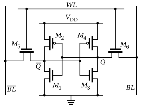
Fig.1 : SRAM Cell
This shows a standard 6T SRAM cell composed of six transistors: two cross-coupled CMOS inverters for data storage and two access transistors controlled by the wordline (WL). The cell stores one bit of data by maintaining complementary internal nodes (Q and QB), while the bitlines (BL and BLB) are used for read and write operations. This structure provides fast access, low static power consumption, and robust data retention, making it the most widely used SRAM cell architecture.
Schematic
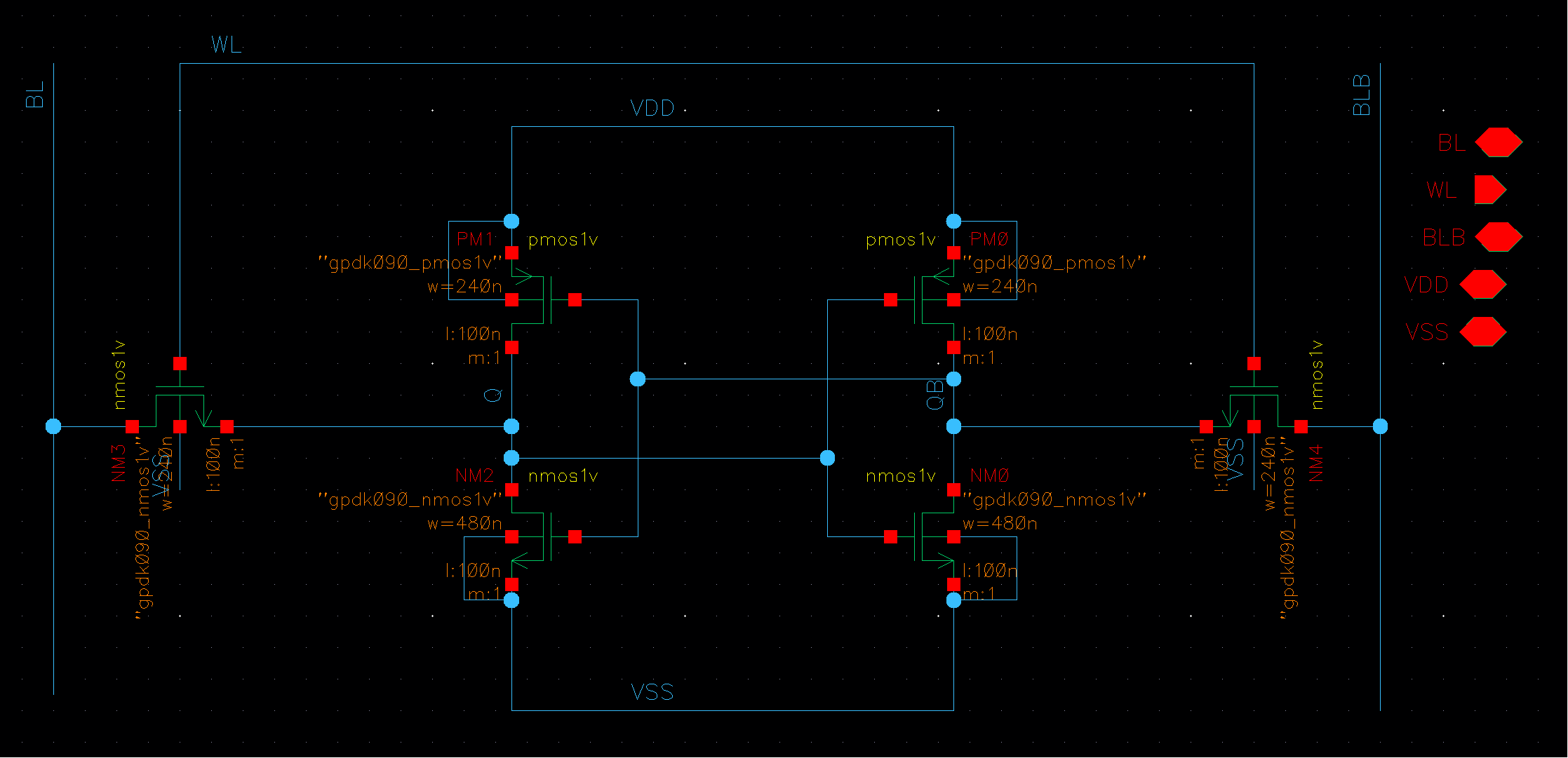
Fig.2 : SRAM Cell Schematic
Based on the standard 6T SRAM architecture, the schematic was implemented using two cross-coupled CMOS inverters and two access transistors. The cell stores data at nodes Q and QB, while BL, BLB, and WL are used for read and write operations.
Functionality Verification
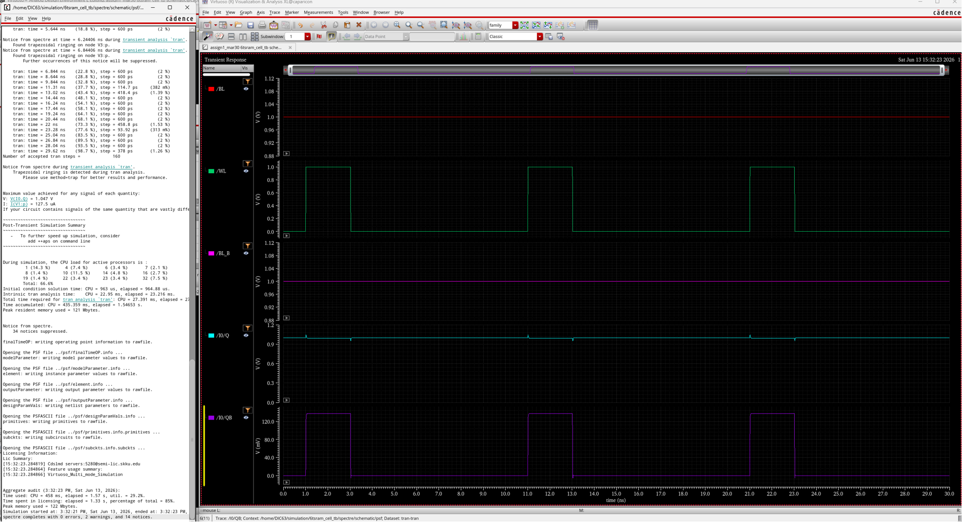
Fig.3 : Read Verification
The read operation was successfully verified, as the stored data remained unchanged during the read access while WL was asserted and both bitlines were precharged to VDD.
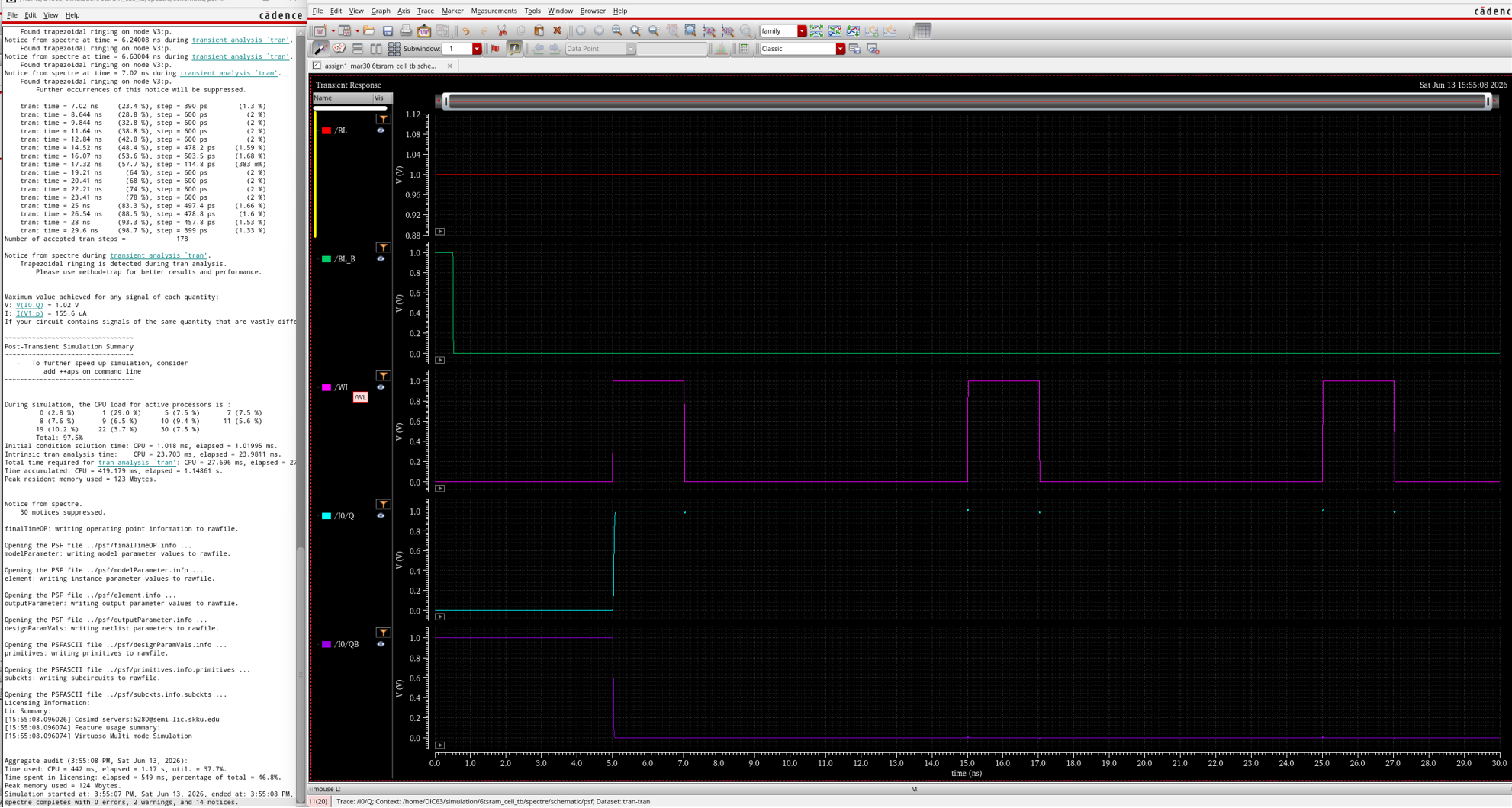
Fig.4 : Write Verification
The write operation was successfully verified, as the stored data changed from (Q, QB) = (1, 0) to (0, 1) when WL was asserted with BL = 0 and BLB = 1.
Static Noise Margin
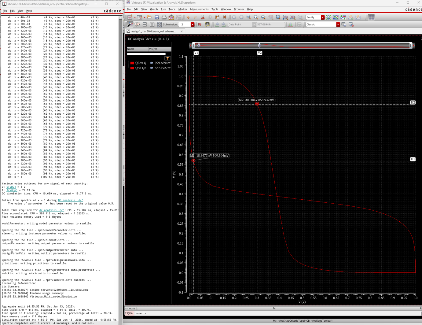
Fig.5 : Static Noise Margin
The hold static noise margin (SNM) of the designed 6T SRAM cell was measured to be approximately 282 mV from the butterfly curve, indicating stable data retention in the hold state.
2. SRAM Column Design
4-to-16 Decoder with Enable Signal
The 4-to-16 decoder is used as the row decoder in the 16×16 SRAM array. Since the array contains 16 rows, four address bits are required to uniquely select one row. The decoder converts the 4-bit row address into one of sixteen wordline signals (WL0–WL15), ensuring that only the selected row is activated during read or write operations. Without the decoder, it would not be possible to access an individual row within the SRAM array. Therefore, the 4-to-16 decoder is an essential component that enables correct row selection and memory access in the 16×16 SRAM design.
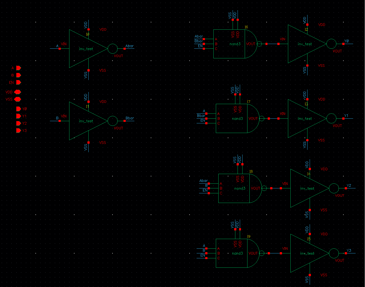
Fig.6 : 2:4 Decoder
As a building block for the 4-to-16 decoder, a 2-to-4 decoder was first designed and implemented. The schematic is shown above.
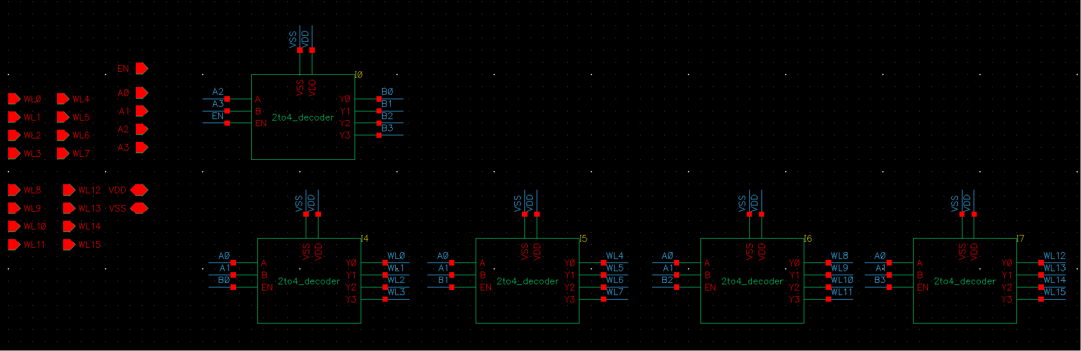
Fig.7 : 4:16 Decoder
To implement the 4-to-16 decoder, a hierarchical structure based on five 2-to-4 decoders was used. As shown in the schematic, the upper 2-to-4 decoder receives the two most significant address bits (A3 and A2) and generates four enable signals (B0–B3). These enable signals are connected to the enable inputs of four lower 2-to-4 decoders. Each lower decoder receives the two least significant address bits (A1 and A0) and generates four wordline outputs. As a result, only one of the sixteen outputs (WL0–WL15) is asserted for a given 4-bit address, realizing a complete 4-to-16 decoding function.
Bit Line Sense Amplifier (BLSA)
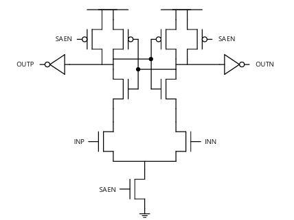
Fig.8 : BLSA
The Bit-Line Sense Amplifier (BLSA) detects a small voltage difference between INP and INN and amplifies it to full-swing digital outputs. When SAEN is low, the sensing circuit is disabled. When SAEN is asserted, the differential input pair converts the input voltage difference into a current difference. The cross-coupled latch then provides positive feedback, rapidly amplifying the small input difference until one output is driven to logic high and the other to logic low. As a result, even a 100 mV input difference can be reliably sensed and converted into complementary outputs (OUTP and OUTN). In an SRAM array, the BLSA is essential because the read operation produces only a small voltage difference on the bitlines, which must be amplified into full-swing digital signals for reliable data sensing.
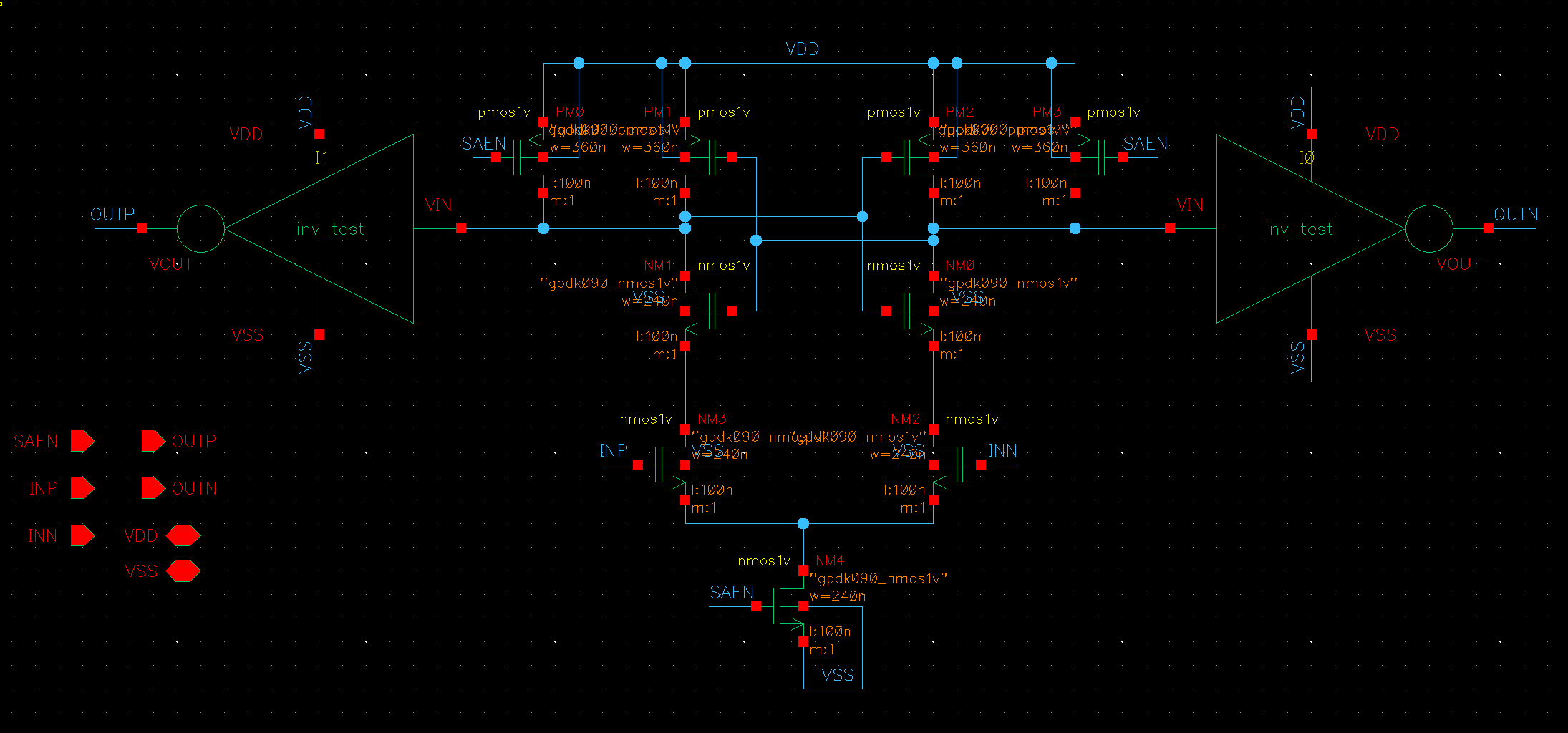
Fig.9 : BLSA Schematic
The BLSA schematic was designed as shown above for reliable sensing of bitline voltage differences in the SRAM array.
Write Driver and Precharge
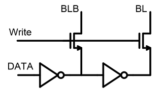
Fig.10 : Write Driver
The write driver is a circuit that drives the bitlines (BL and BLB) with complementary data values during a write operation. As shown above, when the Write signal is asserted, the write driver forces BL and BLB to opposite logic levels according to the input DATA, allowing the selected SRAM cell to be overwritten with the new value.
In an SRAM array, the write driver is essential because the cross-coupled inverters inside the SRAM cell are designed to strongly hold their stored data. Therefore, the bitlines must be actively driven to the desired logic levels with sufficient strength to overcome the stored value and successfully write new data into the selected cell. Without a write driver, reliable write operations would not be possible.
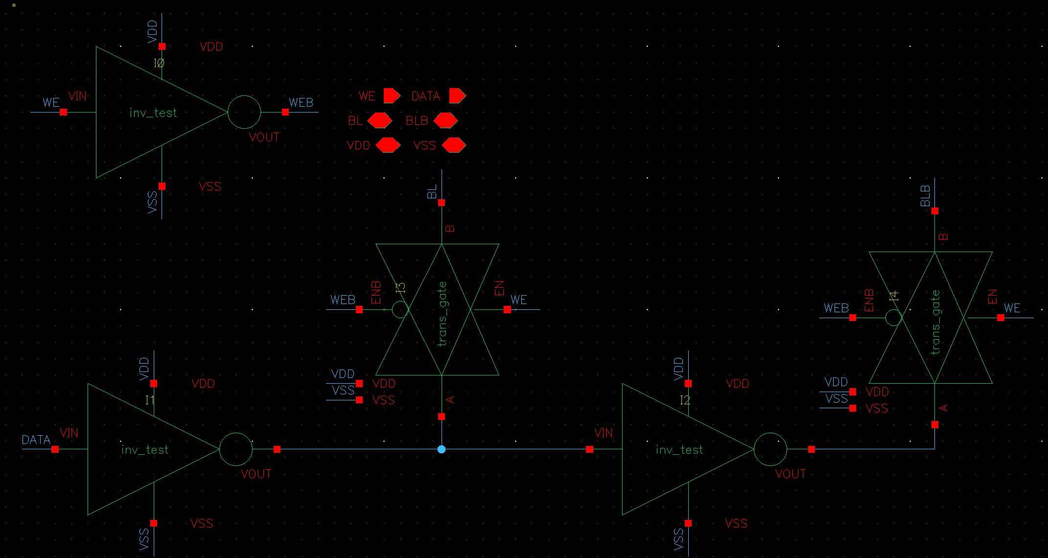
Fig.11 : Write Driver Schematic
Instead of using a single NMOS pass transistor, transmission gates were employed in the write driver to achieve full voltage swing on the bitlines. A single NMOS suffers from a threshold-voltage drop when passing a logic high level, resulting in a degraded output voltage. In contrast, a transmission gate combines an NMOS and a PMOS, enabling both strong logic ‘1’ and strong logic ‘0’ transmission. Therefore, the proposed design can drive BL and BLB closer to the full VDD and GND levels, improving write reliability.
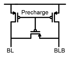
Fig.12 : Precharge Circuit
The precharge circuit initializes both bitlines (BL and BLB) to VDD and equalizes their voltages before a read operation. When the Precharge signal is asserted, both bitlines are charged to the same voltage level. In an SRAM array, the precharge circuit is essential because it provides a known initial condition for the bitlines, allowing the sense amplifier to accurately detect the small voltage difference generated during a read operation.
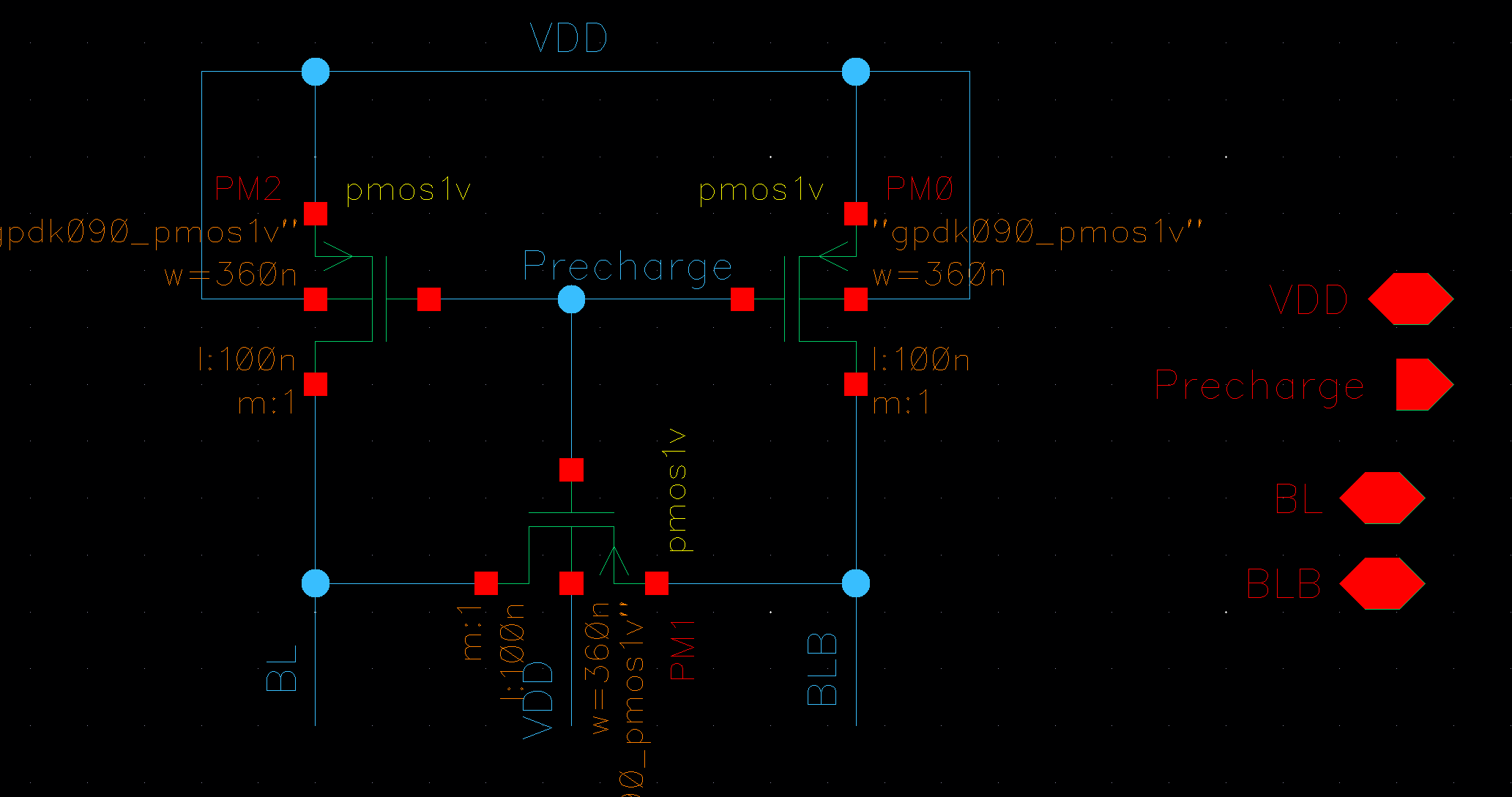
Fig.13 : Precharge Schematic
The precharge circuit shown above was designed to precharge and equalize BL and BLB before each read operation, enabling reliable sensing in the SRAM array.
1 Column with 16bit SRAM cell
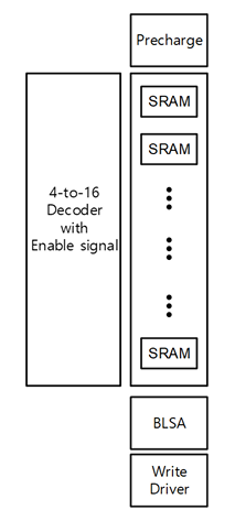
Fig.14 : SRAM Column
As shown in the figure, a single SRAM column consists of several key components:
4-to-16 Decoder: Selects one of the sixteen wordlines (WLs) based on the input address. SRAM Cells: Sixteen 6T SRAM cells are connected vertically in the column. Each cell shares the same bitline pair (BL and BLB) but has a different wordline.
Precharge Circuit: Precharges and equalizes BL and BLB before every read operation.
Write Driver: Drives BL and BLB with complementary data values during write operations. Bit-Line Sense Amplifier (BLSA): Detects and amplifies the small voltage difference developed on BL and BLB during read operations.
During operation, the decoder activates a single wordline, allowing one SRAM cell to communicate with the shared bitlines. The write driver is used for write operations, while the BLSA is used for read operations.
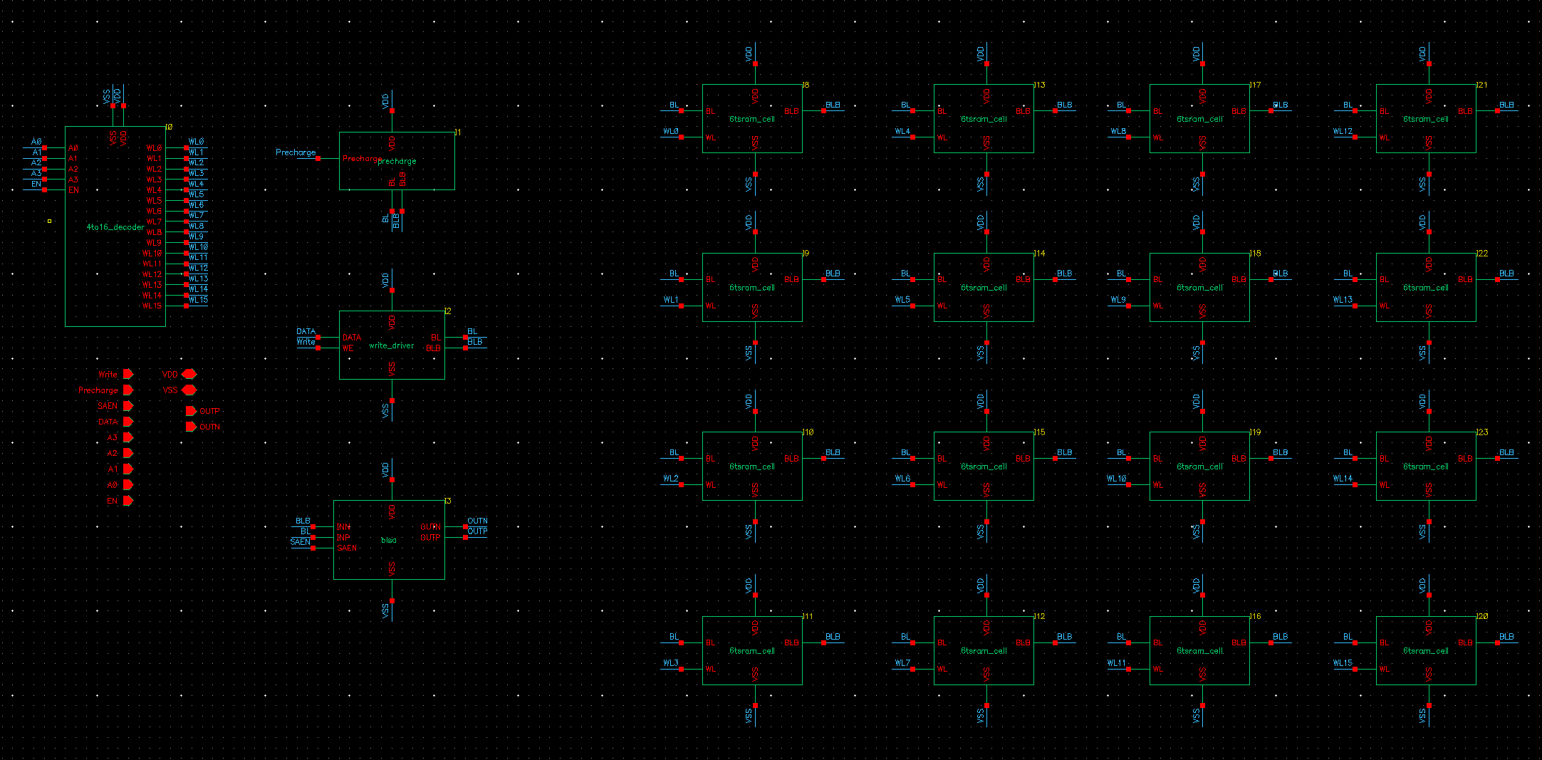
Fig.15 : SRAM Column Schematic
The SRAM column circuit shown above was designed.
Functionality Verification
Write functionalify verification (write 0→1→0→1 .. )
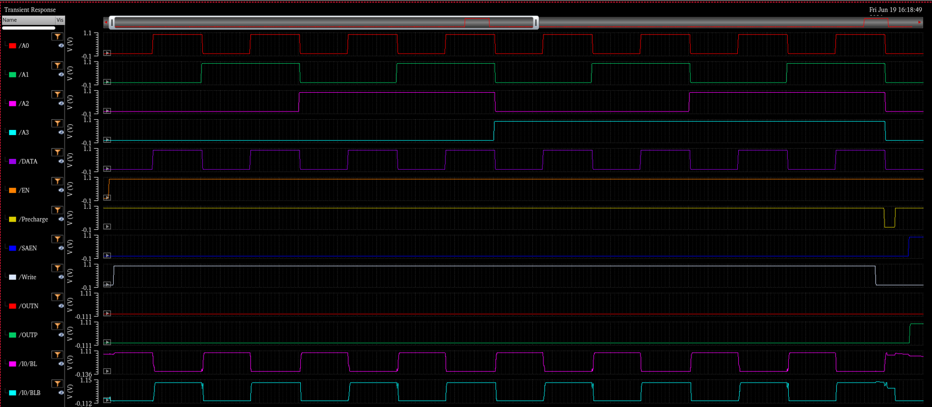
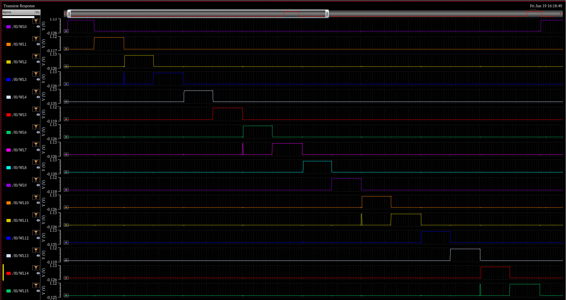
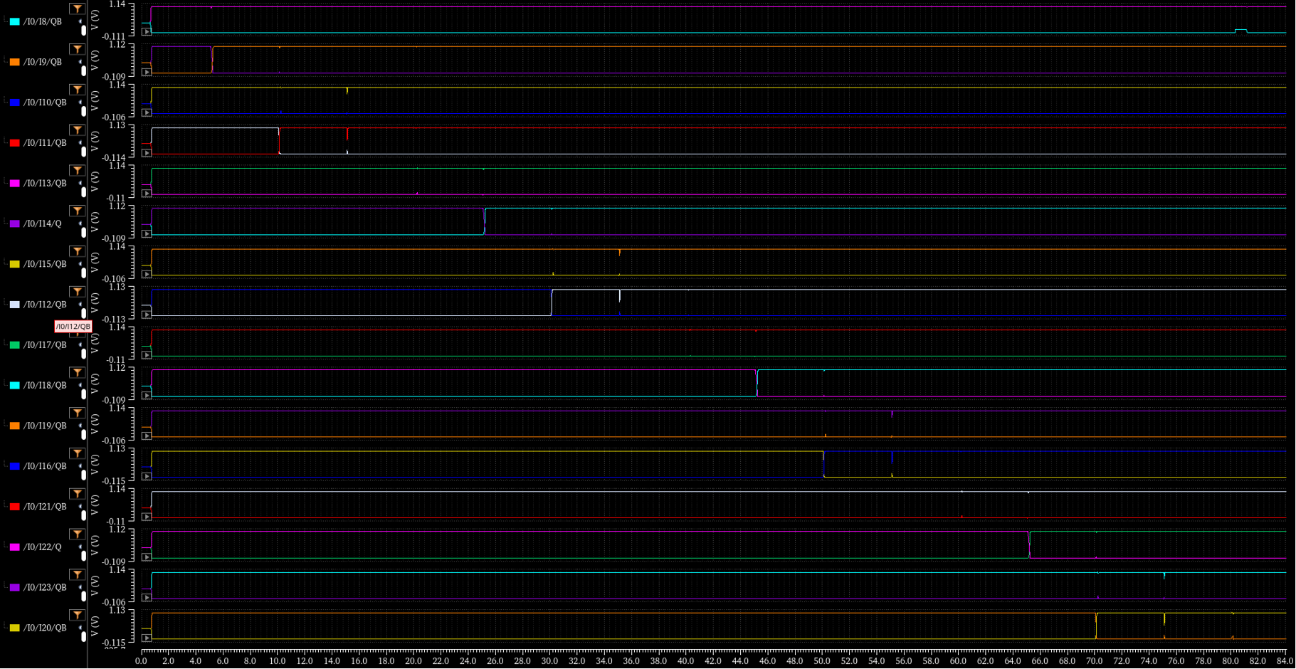
Fig.19-21 : SRAM Column WRITE
The column write operation was verified using the three transient simulation results shown above.
In the first waveform, the outputs of the 4-to-16 decoder (WL0–WL15) are monitored. As the address inputs A3, A2, A1, A0 change sequentially, only one wordline is asserted at a time, confirming correct row selection during the write operation.
The second waveform shows the internal storage nodes (Q and QB) of the SRAM cells in the selected column. Whenever a wordline is activated and the write driver applies the input data to BL and BLB, the corresponding SRAM cell changes its stored value. The complementary behavior of Q and QB confirms that the selected cell is successfully written while the unselected cells retain their previous states.
The third waveform shows the address signals, DATA input, control signals, bitline voltages (BL and BLB), and sense amplifier outputs. During each write cycle, BL and BLB are driven to complementary values according to DATA by the write driver. The selected SRAM cell captures the new value through the activated wordline. The bitline transitions match the intended DATA pattern, demonstrating that the write driver, decoder, and SRAM cell operate correctly together.
Therefore, the three simulation results verify that the column can correctly select a target row, drive the bitlines with the desired data, and successfully store the new value in the selected SRAM cell during write operations.
Write functionalify verification (write 1→0→1→0 .. )
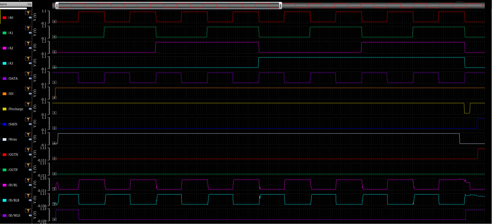
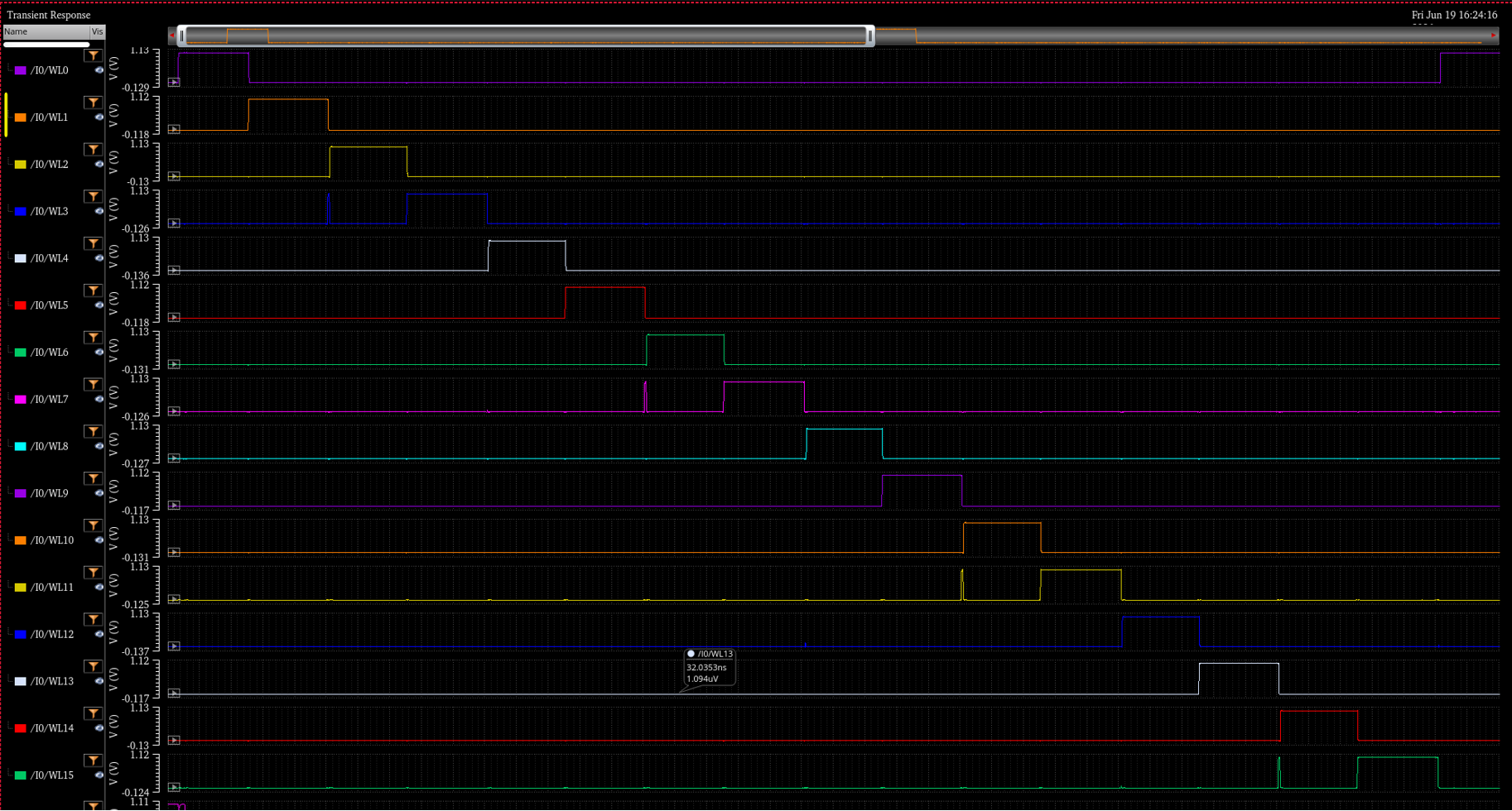
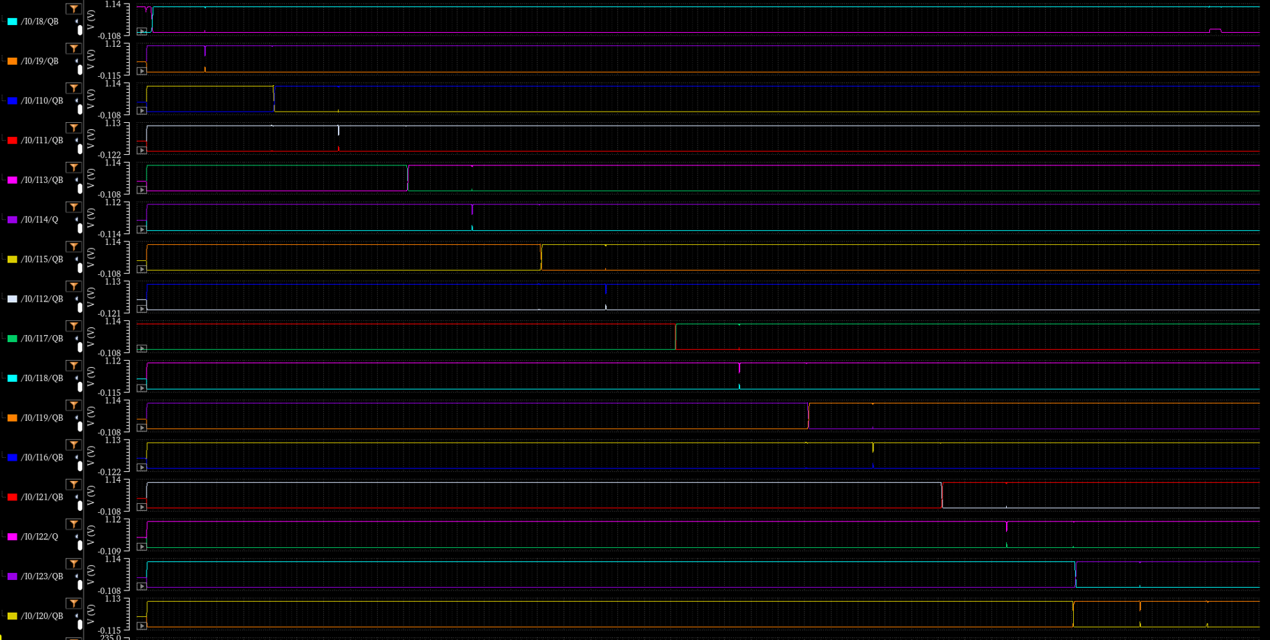
Fig.16-18 : SRAM Column WRITE
The write operation was verified using the three waveforms shown above. The decoder waveform confirms that only one wordline (WL0–WL15) is activated at a time according to the address inputs. The BL and BLB waveforms show complementary bitline voltages driven by the write driver based on the DATA input. Finally, the Q and QB waveforms demonstrate that the selected SRAM cell successfully stores the written value while maintaining complementary logic states. These results confirm correct operation of the decoder, write driver, and SRAM cells during column write operations.
Read Functionality Verification
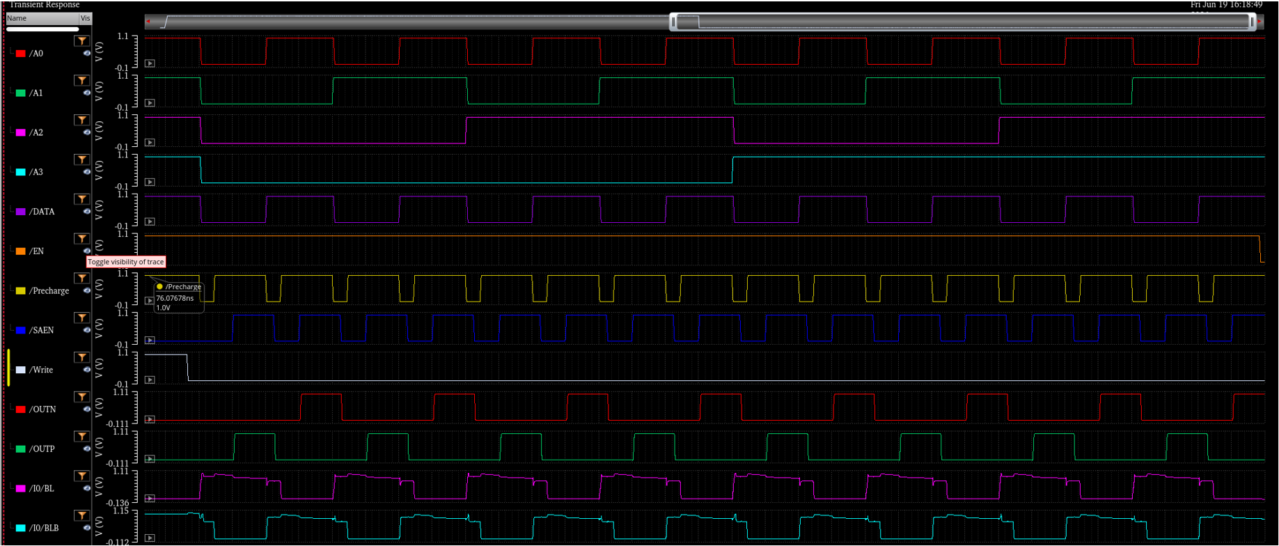
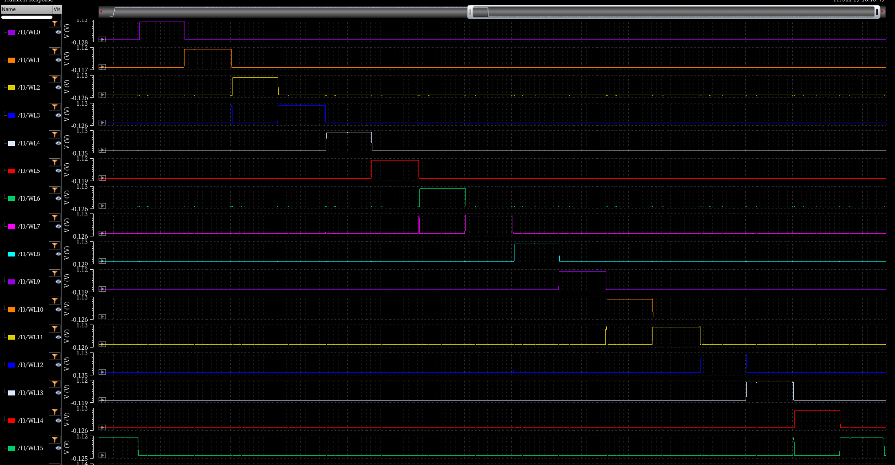
Fig.22-23 : SRAM Column READ
The read operation was verified using the waveforms shown above. The decoder outputs confirm that only one wordline (WL0–WL15) is activated at a time according to the address inputs. During each read cycle, the selected SRAM cell creates a small voltage difference between BL and BLB after precharge. When SAEN is asserted, the BLSA senses this differential voltage and amplifies it to full-swing outputs (OUTP and OUTN). The output waveforms correctly correspond to the data stored in the selected SRAM cells, confirming successful read operation of the SRAM array.
3. 16x16 SRAM Array Design
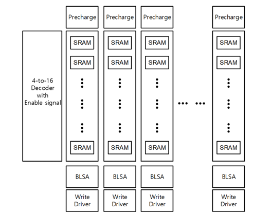
Fig.24 : SRAM Array
This figure illustrates the overall architecture of the 16×16 SRAM array. A single 4-to-16 decoder is shared across all columns to generate the wordlines, while each column contains 16 SRAM cells connected to a dedicated precharge circuit, write driver, and BLSA. The array was designed by replicating the single-column SRAM structure sixteen times, enabling storage and access of 16-bit words in parallel.
Schematic
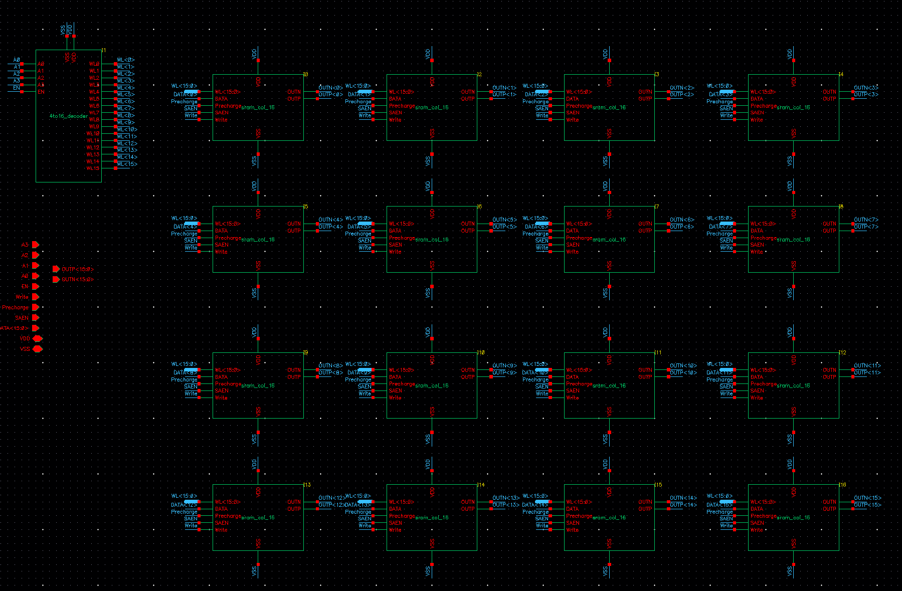
Fig.25 : SRAM Array Schematic
The complete 16×16 SRAM array schematic was implemented as shown above. A single 4-to-16 decoder generates the wordline signals shared by all columns, while sixteen identical SRAM columns are instantiated in parallel. Each column contains a 16-cell SRAM array, a precharge circuit, a write driver, and a BLSA, enabling parallel storage and access of 16-bit data.
Functionality Verification
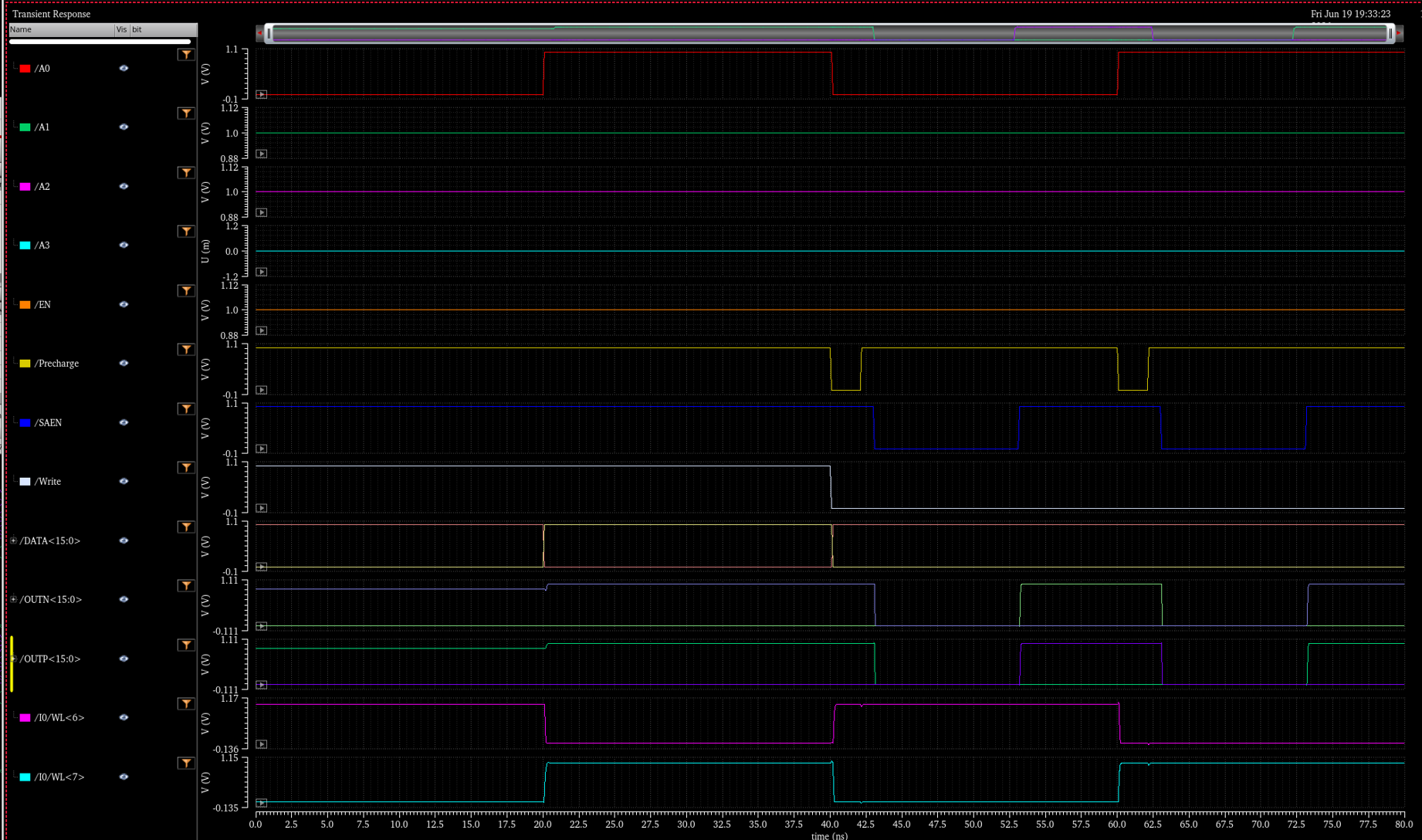
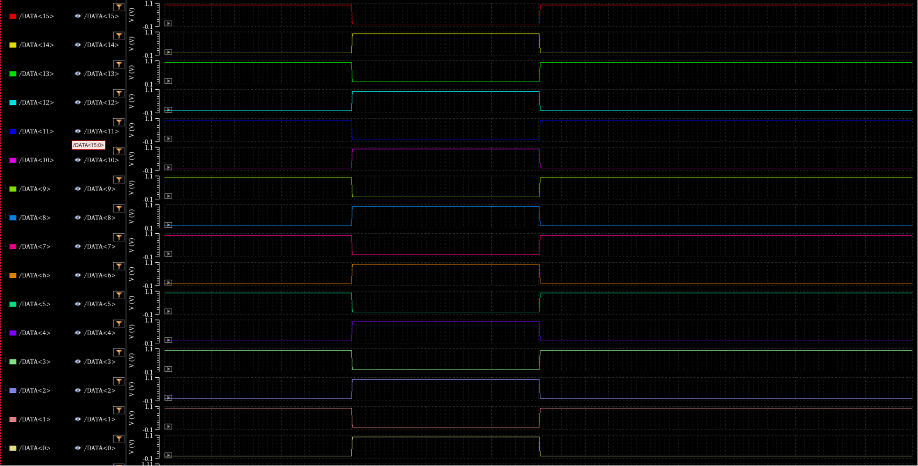
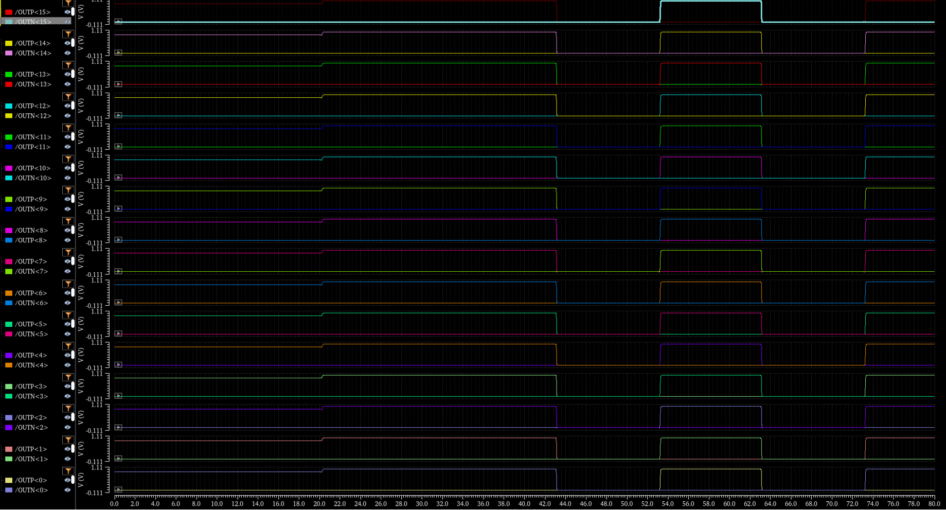
Fig.26-28 : SRAM Array READ & WRITE Verification
To verify the functionality of the proposed 16×16 SRAM array, two rows, WL6 and WL7, were selected for write and read operations. First, the data pattern 1010101010101010 (0xAAAA) was written into WL6, followed by the complementary pattern 0101010101010101 (0x5555) written into WL7. During the write cycles, the selected wordline was activated and the write driver forced the bitlines according to the input data, causing the corresponding SRAM cells to update their stored values. As a result, WL6 and WL7 successfully stored different 16-bit data patterns.
For the read operation, the bitlines were precharged to VDD, after which the selected wordline generated a small voltage difference between BL and BLB depending on the stored data. When the SAEN signal was asserted, the BLSA amplified this differential voltage and produced full-swing output signals. The read results matched the data previously written into WL6 and WL7, confirming successful data storage and retrieval. These results verify the correct operation of the decoder, write driver, precharge circuit, SRAM cell array, and BLSA as an integrated 16×16 SRAM array.
4. Layout
SRAM Cell
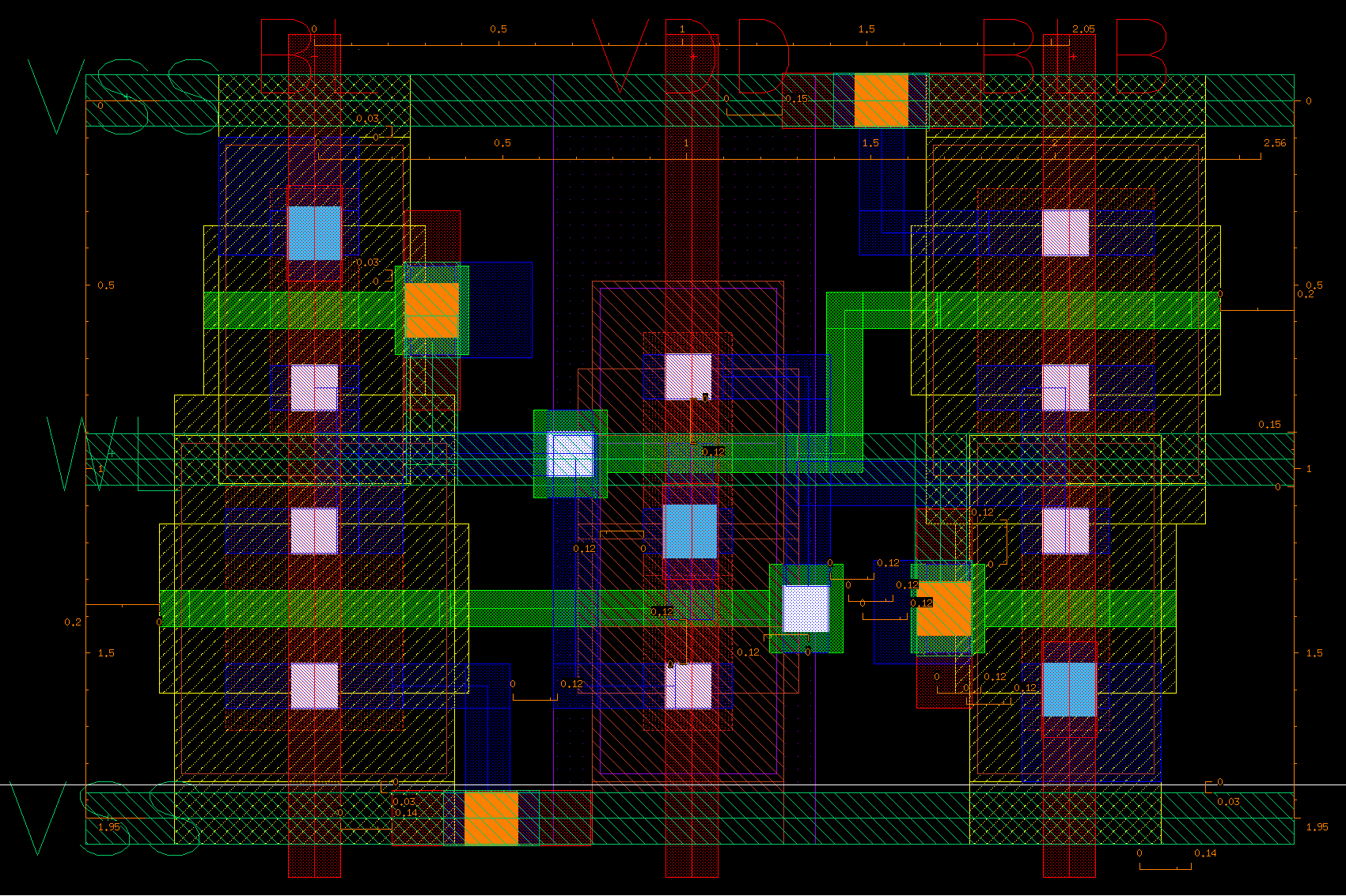
Fig.29 : SRAM Cell Layout
The designed SRAM cell occupies an area of 2.05μm×1.95μm, resulting in a total cell area of 3.9975μm2.
Body Tap Cell
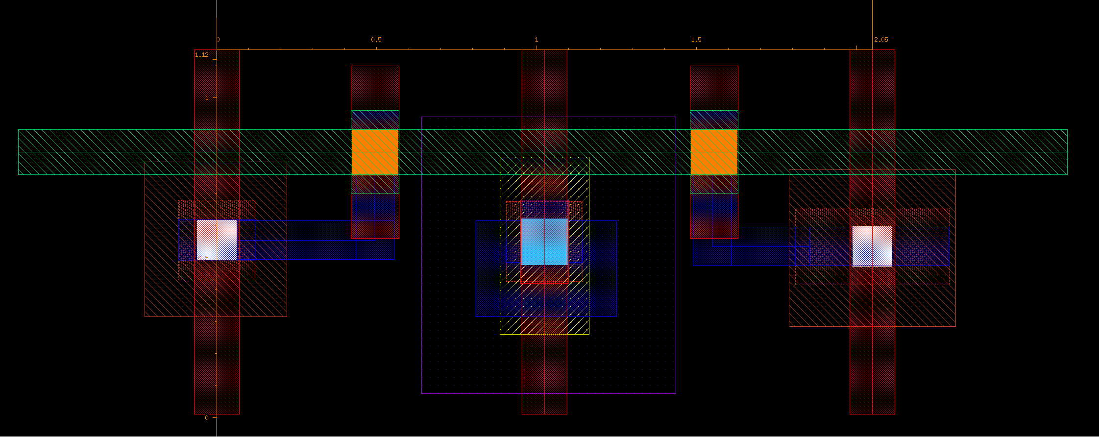
Fig.30 : Body Tap Cell Layout
This figure shows the layout of the body tap cell used in the SRAM array. The body tap cell provides a direct connection between the transistor bodies and the power rails (VDD and VSS), ensuring proper body biasing and preventing latch-up. In the overall layout, body tap cells are inserted periodically to maintain substrate and well potentials.
4-to-16 Decoder
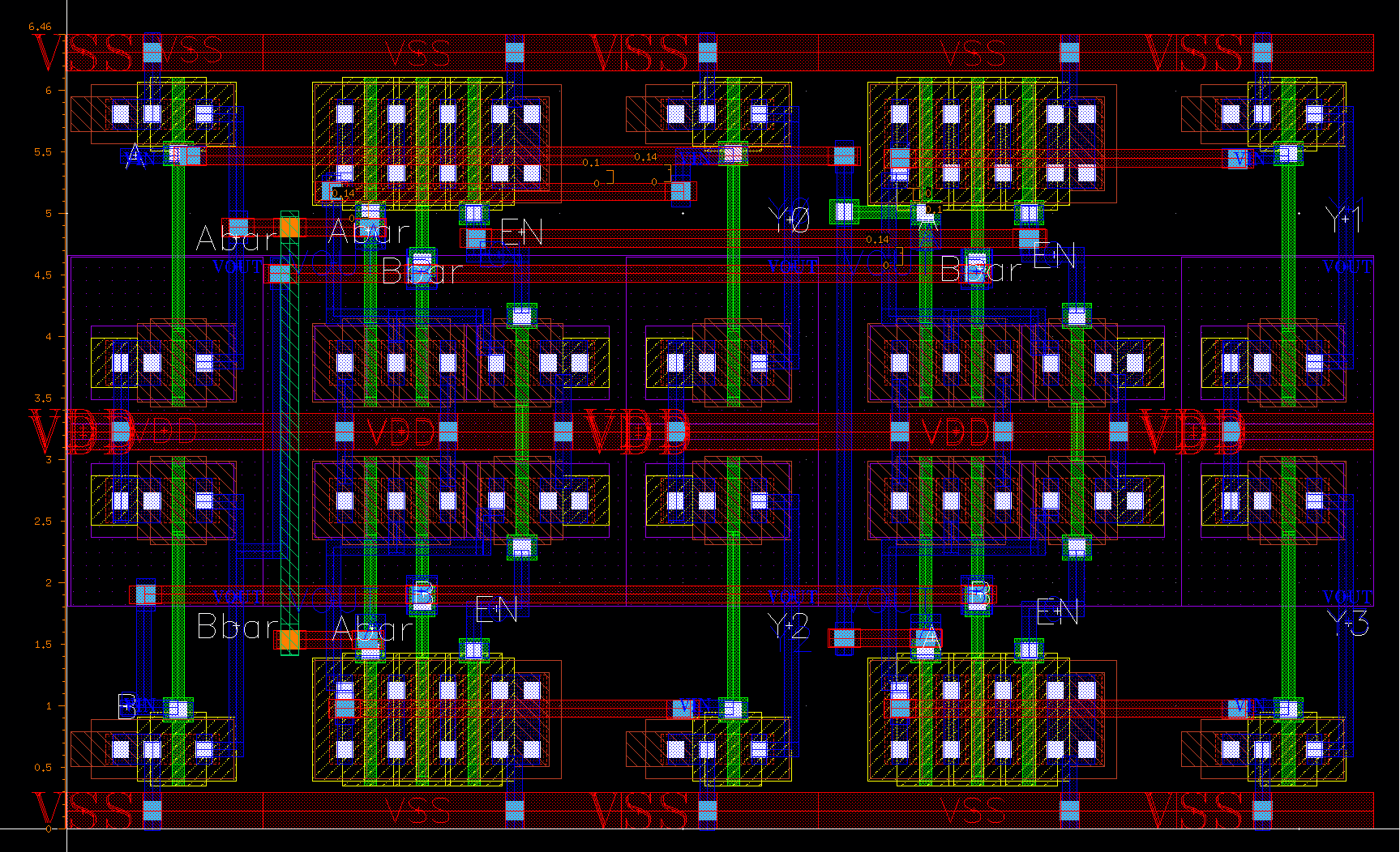
Fig.31 : 2-to-4 decoder Layout
This figure shows the layout of 2-to-4 decoder.
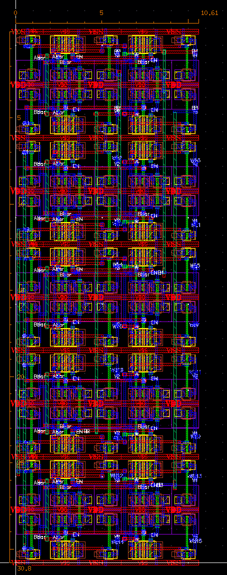
Fig.32 : 4-to-16 decoder Layout
4-to-16 decoder was designed, based on the 2-to-4 decoder layout.
BLSA
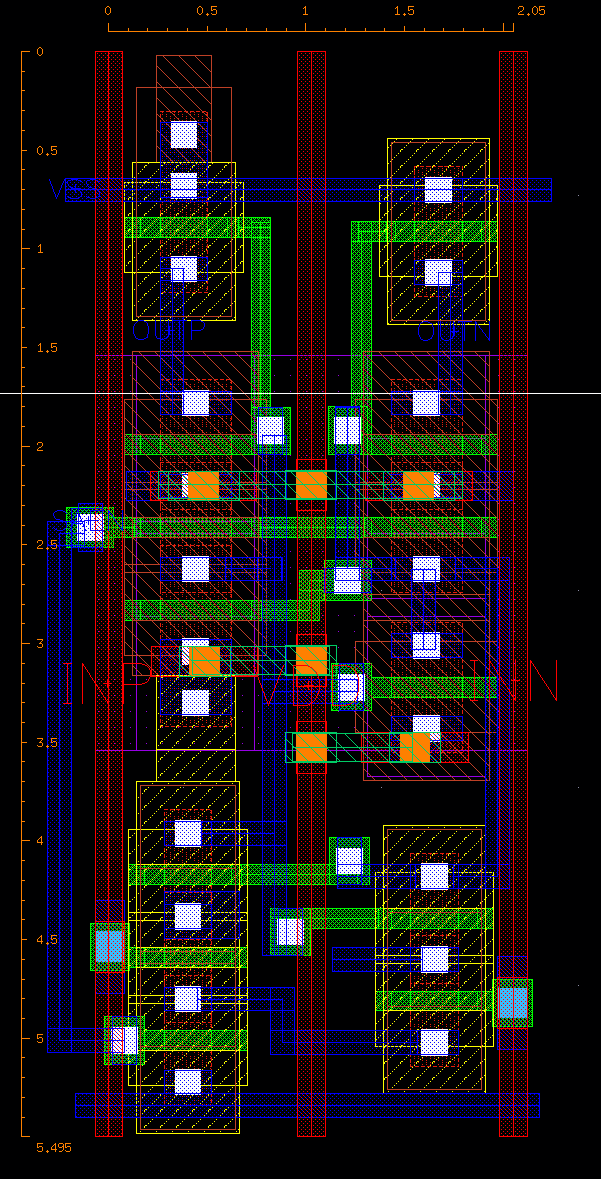
Fig.33 : BLSA Layout
This figure shows the layout design of BLSA. The width of the designed layout is identical to that of SRAM cell.
Write Driver
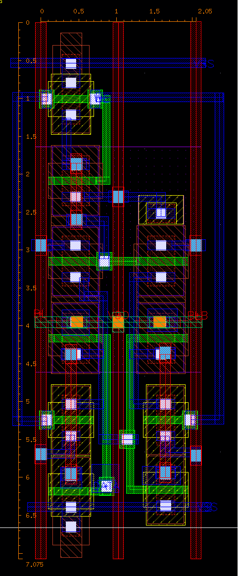
Fig.34 : Write Driver Layout
This figure shows the layout design of write driver. The width of the designed layout is identical to that of SRAM cell.
Precharge
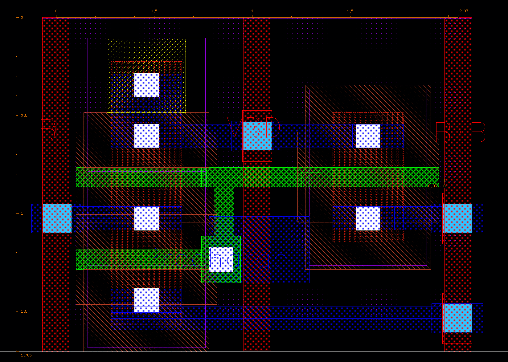
Fig.35 : Precharge Layout
This figure shows the layout design of precharge circuit. The width of the designed layout is identical to that of SRAM cell.
1 column with 16bit SRAM

Fig.36 : 1 Column with 16bit SRAM Layout
This figure shows the layout design of SRAM column. For one column, the body tap cells were inserted at the top, in the middle, and at the bottom to prevent latch-up.

Fig.37 : 1 Column with Peripheral Circuits Layout
This figure shows the layout design of SRAM 1 column, with peripheral circuits such as precharge, BLSA and write driver.
16x16 SRAM Array
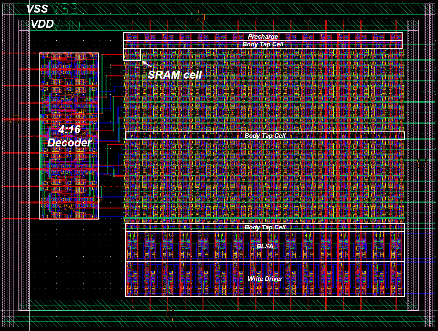
Fig.38 : SRAM array Layout
The final layout implementation of the 16×16 SRAM array, including the decoder, SRAM cells, precharge circuits, write drivers, BLSAs, and body tap cells, is shown above.