[tape-out project] quantized BC-ResNet models for keyword spotting and speaker verification
Published:
This post details the design and implementation of a quantized BC-ResNet-based neural network accelerator for keyword spotting (KWS) and speaker verification (SV), culminating in a successful ASIC tape-out using Samsung’s 28 nm LPP process. The project demonstrates a hardware–software co-design approach, achieving low power consumption and high accuracy for edge audio intelligence applications.
1. Introduction
The demand for AI processors has been rapidly increasing as machine learning applications continue to expand into edge and IoT devices. Among them, keyword spotting (KWS) and speaker verification (SV) systems have become fundamental components in modern voice-based human–machine interfaces, such as smart speakers, mobile assistants, and wearable devices. These systems enable always-on, low-power auditory perception, allowing devices to respond to wake words or authenticate users through voice features without relying on cloud processing.
In this research project, we aim to tape out a low-power AI processor, exploiting the synergy between neural model compression and hardware optimization for embedded audio intelligence.
2. Related Work
Tan et al. (JSSC 2025) [1] present a 1.8% FAR, 2 ms decision-latency SV-assisted KWS chip in 28 nm CMOS. They propose a transfer-computing model that shares convolutional layers between KWS and SV, cutting MACs and parameters by ≈1.8×. A hybrid-IF-domain circuit processes analog and digital features to eliminate ADC overhead, and a scalable 5T-SRAM reduces read/leakage power by >10×. The chip achieves 91.8 % accuracy, 1.73 nJ/decision, and 1.73 µW active power, which is the lowest among prior KWS ASICs
Xiao et al. (ISSCC 2024) [2] introduce KASP, a 55 nm KWS + SV processor using adaptive beamforming, direction-of-arrival estimation, and progressive wake-up to suppress human-voice noise. Its Lite-FDBF and Lite-X-Vector SV enable multi-user verification without speaker-specific training, reducing MACs by 99.7 % with only 1.4 % accuracy loss. KASP achieves 96.8 % KWS accuracy and 1.68 µJ/classification, representing a major advance in noise-robust, ultra-low-energy speech interfaces.
Unlike prior works, our work introduces a fully digitized computation and model architecture that enhances accuracy while leveraging early-exiting branches to reduce the switching activity of power-hungry digital cells, thereby achieving lower overall power consumption.
3. System Overview
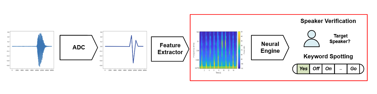
Fig. 1 : Overall System Pipeline
The overall system pipeline, as illustrated in Fig. 1, consists of three main components: an Analog-to-Digital Converter (ADC), a Feature Extractor, and a Neural Engine.
First, the incoming acoustic waveform is captured and digitized through the ADC, which converts the continuous analog speech signal into quantized digital samples suitable for further digital processing. These quantized signals are then passed to the Feature Extractor, which computes time–frequency representations such as Mel-spectrograms to capture the spectral characteristics of the speech signal.
The extracted features are subsequently fed into the Neural Engine, which performs two parallel inference tasks: Keyword Spotting (KWS) and Speaker Verification (SV). The neural network identifies whether the spoken utterance corresponds to a predefined keyword and simultaneously verifies whether the detected voice matches a registered target speaker.
In this project, the Neural Engine (highlighted in the red box of Fig. 1) was fully implemented, including model quantization, digital inference pipeline, and hardware mapping. The ADC and Feature Extractor modules were developed by collaborating teams and interfaced with the neural engine for end-to-end system evaluation.
4. Model Design
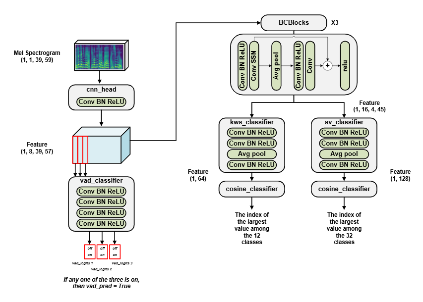
Fig. 2 : Model Design
The proposed model architecture is based on BC-ResNet, which is known for its parameter efficiency and suitability for embedded speech applications. The original BC-ResNet consists of three main components: a CNN head, a sequence of BCBlocks, and a Classifier. To jointly handle Voice Activity Detection (VAD), Keyword Spotting (KWS), and Speaker Verification (SV) within a unified framework, the architecture was modified as shown in Fig. 2.
The input Mel-spectrogram (dimension: 1 × 1 × 39 × 59) is first processed by the CNN head, which performs initial feature extraction using convolution, batch normalization, and ReLU activation. From this output, the first three time steps of the feature map are directed to the VAD classifier, composed of four sequential convolutional blocks (Conv–BN–ReLU). If any of the three VAD logits indicate activity (i.e., vad_pred=True), the subsequent processing stages are activated.
In the next stage, the complete feature map is passed through three stacked BCBlocks, each consisting of a Conv–BN–ReLU, Conv–SSN (Sub-Spectral Normalization), Average Pooling, and an additional Conv–BN–ReLU sequence, with skip connections to preserve feature continuity and mitigate gradient degradation. These BCBlocks extract compact, discriminative embeddings suitable for both KWS and SV.
The resulting features are branched into two task-specific heads: the KWS classifier and the SV classifier. Each classifier comprises a shallow Conv–BN–ReLU stack followed by an average pooling layer, producing embedding vectors of size (1, 64) for KWS and (1, 128) for SV, respectively. These embeddings are then passed to cosine classifiers, which compute similarity scores between the embeddings and class prototypes. The index of the maximum cosine similarity determines the predicted keyword or speaker identity. For the ASIC implementation, only the neural encoder portion up to the embedding vector output was realized, while the cosine classifier was executed in software.
Quantization Setup
Quantization-aware training (QAT) was applied to reduce model precision while maintaining accuracy. Both weights and activations were quantized to 8 bits (W8A8), with 32-bit accumulations for residual connections. Each Conv–BN–ReLU and Conv–SSN pair was fused into a single quantized operation to minimize computational overhead. All layers, including AdaptiveAvgPool2d, Fully Connected, Convolution, and Residual paths, were quantized to ensure full-integer arithmetic compatibility for hardware deployment. Per-channel scaling was applied to improve numerical stability during training and inference.
Training Environment
The model was trained on the Google Speech Commands v2 (GSCD) dataset using the SGD optimizer with a momentum of 0.9 and a weight decay of 1 × 10⁻³. The total number of epochs was 300, including a 10-epoch warmup phase. The initial learning rate was set to 1.2 × 10⁻² and decayed to a lower limit of 2 × 10⁻⁵ following a cosine schedule.
Loss functions were defined using AAM-Softmax, with task-specific weighting parameters:
- SV loss (\(\lambda_{sv} = 0.3\))
- KWS loss (\(\lambda_{kws} = 0.25\))
- VAD loss (\(\lambda_{vad} = 1.0\))
Formally, the total training objective was expressed as:
\[\mathcal{L}_{total} = \lambda_{vad}\mathcal{L}_{vad} + \lambda_{kws}\mathcal{L}_{kws} + \lambda_{sv}\mathcal{L}_{sv}\]where \(\mathcal{L}_{kws}\) and \(\mathcal{L}_{sv}\) were computed using \(\operatorname{AAMSoftmaxLoss}(\text{num_classes}, \text{num_emb_dim})\) for 64- and 256-dimensional embeddings, respectively.
5. Hardware Design
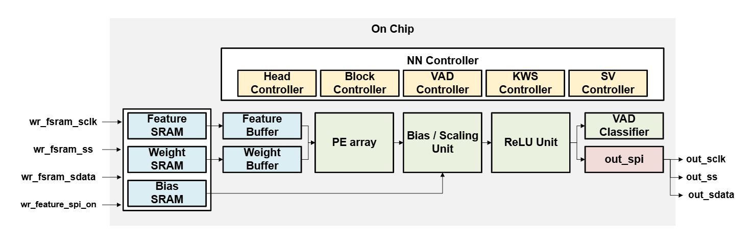
Fig. 3 : Hardware Architecture
The proposed hardware architecture, illustrated in Fig. 3, implements the quantized BC-ResNet model for real-time keyword spotting (KWS), speaker verification (SV), and voice activity detection (VAD). The design follows a hardware–software co-design methodology, where the quantized model described in Section 4 is mapped to a custom fixed-point inference accelerator optimized for low-power edge operation.
5.1 Architecture Overview
The entire system is implemented on-chip, consisting of a Neural Network (NN) Controller, multiple on-chip SRAM modules, a Processing Element (PE) array, and dedicated functional units. The NN Controller is hierarchically organized into submodules: Head Controller, Block Controller, VAD Controller, KWS Controller, and SV Controller, each responsible for orchestrating the corresponding layer group in the neural network.
The Feature, Weight, and Bias SRAMs store the quantized feature maps, model parameters, and biases, respectively. Each SRAM is connected to a corresponding buffer to decouple memory access from computation and enable parallel data streaming. The PE array performs core multiply–accumulate (MAC) operations, and its output passes through a Bias/Scaling Unit and a ReLU Unit before being written back to SRAM or sent to the classifier. The VAD Classifier produces the final decision, which is transmitted via an SPI interface (out_sclk, out_ss, out_sdata).
5.2 Dataflow Strategy
The accelerator employs a channel-wise (output-stationary) dataflow, where each PE is assigned to one output channel. A total of 16 PEs operate in parallel, each accumulating partial sums locally to minimize memory access overhead. The weight and feature buffers are double-buffered to enable concurrent data loading and computation, ensuring high utilization of the PE array.
This approach strikes a balance between compute efficiency and memory bandwidth, as weights remain stationary within the PEs while features are streamed from the Feature Buffer during each convolutional cycle.
5.3 Fixed-Point Arithmetic Implementation
All arithmetic operations are performed in fixed-point precision to reduce area and power consumption.
- Input to PE: 8-bit feature and 8-bit weight operands
Output of PE: 21-bit accumulation result
The accumulated value is then processed by the Bias/Scaling Unit, which applies per-channel scaling and bias correction to restore dynamic range. The scaled result passes through the ReLU Unit, where rounding and saturation are applied. Since ReLU6 activation is adopted, the output is saturated at a maximum value of 6, preventing numerical overflow while preserving nonlinear activation effects.
5.4 Memory Design
The on-chip memory subsystem consists of three dedicated SRAM blocks:
- Feature SRAM (64 KB) – stores intermediate activation maps
- Weight SRAM (128 KB) – holds quantized model parameters
- Bias SRAM (16 KB) – retains bias and scale coefficients
Data are transferred from the SRAMs to their respective buffers through an SPI-based write interface (wr_fsram_sclk, wr_fsram_ss, wr_fsram_sdata). The buffered memory architecture minimizes memory access latency and enables concurrent read/write operations for pipelined computation. Bandwidth analysis confirmed that the system sustains continuous dataflow at the operating frequency without stalling, even under multi-branch execution.
5.5 Clock Gating and Power Optimization
To achieve low power consumption, fine-grained clock gating was applied to idle submodules such as inactive controllers or PEs. The system dynamically disables unused PEs during lightweight tasks (e.g., VAD), reducing dynamic power dissipation. The Bias/Scaling Unit and ReLU Unit also employ operand-aware gating, activating only when valid data are available. This technique, combined with SRAM access scheduling, effectively minimizes unnecessary switching activity across the datapath.
6. ASIC Implementation
The quantized neural-network accelerator was implemented using the Samsung 28 nm Low-Power Plus (LPP) CMOS process. The full physical design flow—from RTL synthesis to place-and-route (P&R), timing closure, and sign-off—was carried out using the Synopsys Design Compiler and IC Compiler II toolchain.
6.1 Layout Overview
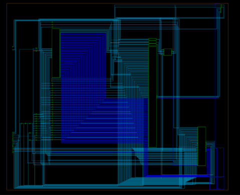
Fig 4. Schematic View of Synthesized Design
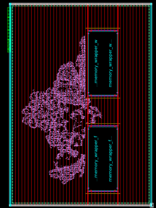
Fig 5. Layout view of the Design
Fig. 4 shows the post-layout view of the accelerator, including the logic and on-chip memory blocks. The core layout integrates three major SRAM macros (feature, weight, and bias memories) and the compute datapath consisting of the PE array, bias/scaling unit, and control logic. The final floorplan (Fig. 5) reveals a compact rectangular structure, with the memory macros placed symmetrically at the top and bottom of the core to minimize routing congestion and interconnect delay between compute and storage units. Metal routing was performed over six layers, and congestion analysis confirmed a utilization below 75 %, ensuring good routability.
6.2 Timing Analysis
Post-layout timing analysis was performed under typical and worst-case process–voltage–temperature (PVT) corners.
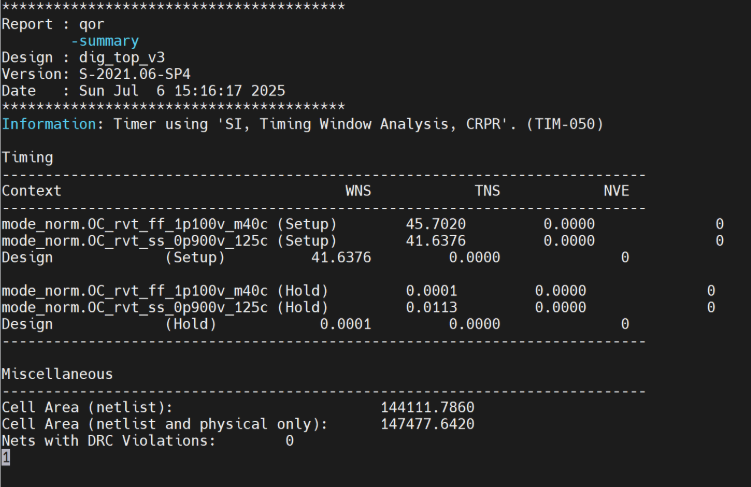
Fig. 6 : qor summary
As summarized in Fig. 6, the design achieved:
- Worst Negative Slack (WNS): 41.6 ps
- Total Negative Slack (TNS): 0 ns
- No setup or hold violations across all operating corners.
This result indicates successful timing closure with sufficient margin for 100 MHz operation under both fast–fast (1.0 V, –40 °C) and slow–slow (0.9 V, 125 °C) conditions.
6.3 Constraint and Rule Verification
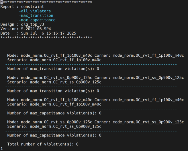
Fig. 7 : Constraint verification reports
Constraint verification reports (Fig. 7) show zero violations for both maximum transition and maximum capacitance checks, confirming that all cell drive strengths and wire loads meet sign-off requirements. No DRC (Design Rule Check) or LVS (Layout Versus Schematic) violations were observed after final extraction, validating geometric and connectivity correctness.
6.4 Area Analysis
The synthesized cell area was 1.44 × 10⁶ µm², and the post-layout area increased slightly to 1.47 × 10⁶ µm² due to placement and routing overhead. The design occupied a core size of approximately 1.2 mm × 1.2 mm, which includes logic, buffers, and interconnect routing channels. The area distribution is dominated by the PE array and memory interfaces, accounting for roughly 70 % of the total area.
6.5 Power Analysis
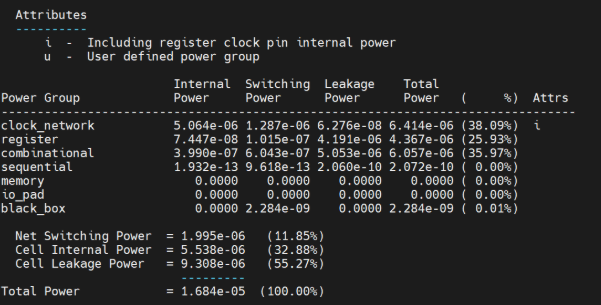
Fig. 8 : Power BreakDown
The post-layout power breakdown obtained from PrimeTime-PX is summarized in Fig. 8.
At nominal operating conditions (0.9 V, 100 MHz):
- Total Power: 1.68 × 10⁻⁵ W (16.8 µW)
- Clock Network: 38.1 %
- Combinational Logic: 35.7 %
- Registers: 25.9 %
- Leakage Power: 55.3 % of total cell power
The relatively high leakage fraction is attributed to always-on logic and dense register networks used in the PE array. However, dynamic power remains low due to the applied clock-gating and operand-aware activation techniques described in Section 5.5.
6.6 Physical Verification and Sign-Off
The final design passed all Design Rule Check (DRC) and Layout Versus Schematic (LVS) verifications without errors. IR-drop and electromigration analyses were also performed, showing voltage droop within ±3 % of the nominal supply. The chip was thus ready for GDSII tape-out submission under the MPW program.
6.7 Summary of Implementation Results
| Metric | Value | Notes |
|---|---|---|
| Process Technology | Samsung 28 nm LPP | Low-Power Plus CMOS |
| Core Area | 1.47 × 10⁶ µm² | Including SRAMs |
| Operating Voltage | 0.9 – 1.0 V | SS/FF corners |
| Max Frequency | 200 kHz | 0 ns TNS |
| Total Power | 16.8 µW | @ 0.9 V, 200 kHz |
| Cell Utilization | 72 % | Post-route |
| DRC/LVS Violations | 0 / 0 | Passed |
| SRAM Macros | 2 | Feature / Weight & Bias |
7. Conclusion
This work presented the design and implementation of a quantized BC-ResNet–based neural network accelerator for keyword spotting (KWS) and speaker verification (SV), realized through a complete ASIC flow using the Samsung 28 nm LPP process. The proposed system adopts a hardware–software co-design approach, combining algorithmic quantization, network architecture optimization, and silicon-level efficiency enhancement to achieve real-time audio inference under strict power and area constraints.
Through quantization-aware training, the model achieved high accuracy while maintaining full 8-bit integer precision (W8A8), enabling seamless hardware mapping without floating-point overhead. The final ASIC demonstrated 16.8 µW total power consumption, a core area of 1.47 × 10⁶ µm², and timing closure at 200 kHz, validating its suitability for always-on, low-power audio processing. The architecture’s hierarchical controller structure and PE-level parallelism further ensured efficient multi-task execution across VAD, KWS, and SV domains.
The key innovations of this work include:
- Integration of BC-ResNet architecture with quantization-aware training for efficient speech embedding generation.
- Implementation of a fully digitized inference engine optimized for integer arithmetic and ReLU6 activation.
- Realization of a multi-task neural accelerator capable of simultaneous voice activity detection and speaker-aware keyword recognition.
This project demonstrates the feasibility of deploying advanced neural models on resource-constrained edge platforms. Beyond this tape-out, future work will focus on post-silicon validation, multi-keyword scalability, and on-chip cosine similarity computation for complete end-to-end inference. The methodology established here provides a foundation for next-generation ultra-low-power AI processors targeting human-centric, always-on intelligence in edge and wearable devices.
8. References
[1] F. Tan, W. -H. Yu, J. Lin, K. -F. Un, R. P. Martins and P. -I. Mak, “A 1.8% FAR, 2 ms Decision Latency, 1.73 nJ/Decision Keywords-Spotting (KWS) Chip Incorporating Transfer-Computing Speaker Verification, Hybrid-IF-Domain Computing and Scalable 5T-SRAM,” in IEEE Journal of Solid-State Circuits, vol. 60, no. 3, pp. 1103-1112, March 2025
[2] J. Xiao et al., “14.8 KASP: A 96.8% 10-Keyword Accuracy and 1.68μJ/Classification Keyword Spotting and Speaker Verification Processor Using Adaptive Beamforming and Progressive Wake-Up,” 2024 IEEE International Solid-State Circuits Conference (ISSCC), San Francisco, CA, USA, 2024, pp. 268-270
Acknowledgment
This research was conducted as part of the Undergraduate Research Program (URP) and supported by the IDEC Multi-Project Wafer (MPW) initiative using Samsung 28 nm CMOS process.