[project] Senior Year Capstone Design : Front-end and Back-end Design of Digital CNN Accelerator for SubPixel Rendering Algorithm
Published:
This project was carried out as a Senior Capstone Design from March to June 2025. It received the Engineering Innovation Prize at the SKKU Senior Capstone Design Contest 2025. I served as the team leader, and my teammates were Somin Kang, Miri Kim, and Jaehwan Shin.
https://github.com/chae-sy/capstone_design

we will present our project titled ‘Subpixel Rendering CNN Accelerator Based on Hardware–Software Co-Design Methodology.
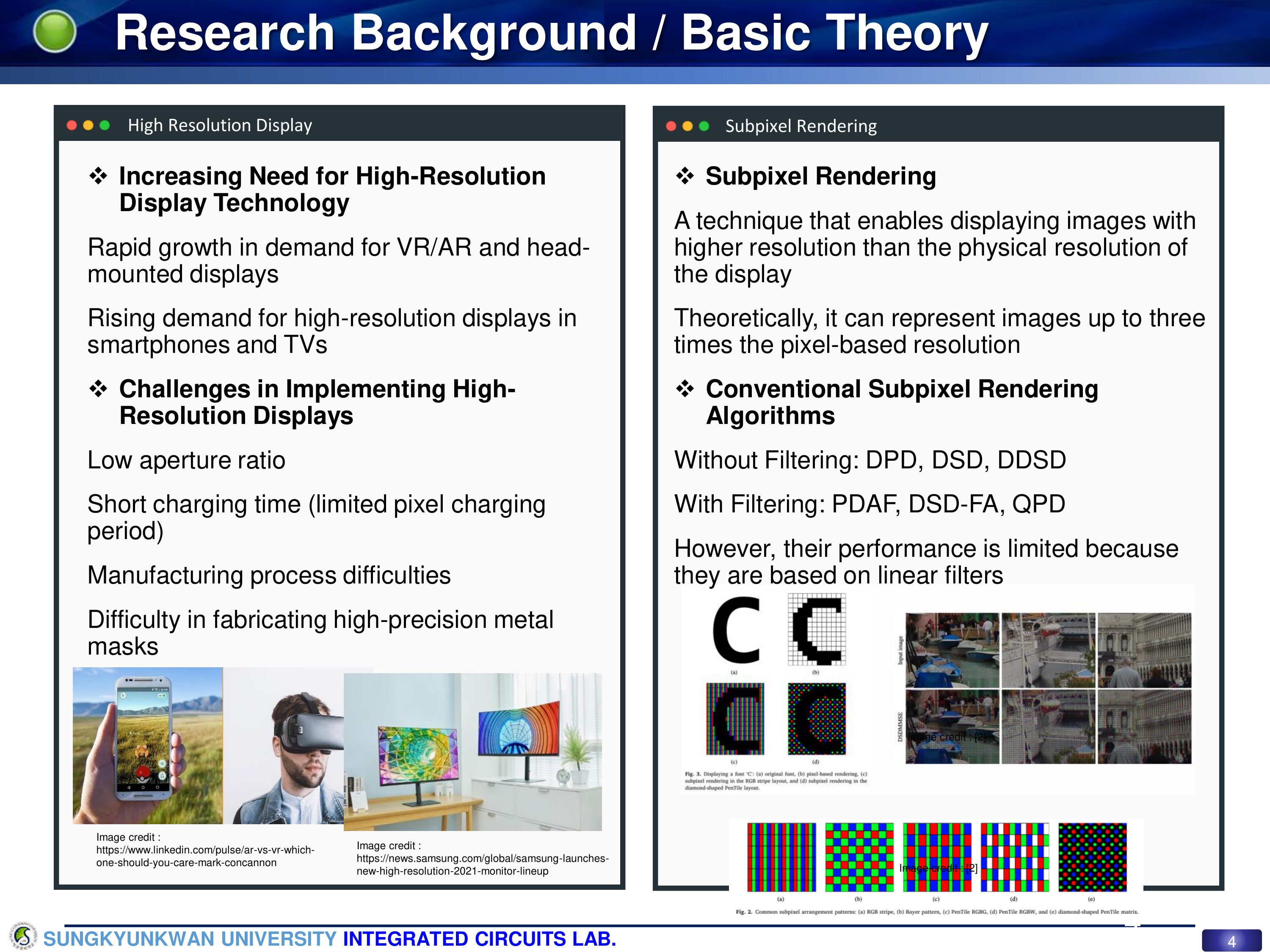
The demand for high-resolution displays continues to grow, yet achieving high-quality visual performance remains challenging due to physical pixel density limits and fabrication constraints.
To overcome these limitations, Subpixel Rendering (SPR) technology enhances perceived resolution by manipulating not only pixels but also individual subpixels
However, conventional filter-based subpixel rendering approaches have inherent performance limitations.
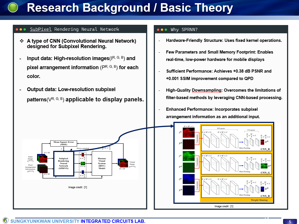
To address this, we adopted a CNN-based model called SPRNN, which learns nonlinear characteristics and improves both PSNR and SSIM metrics.
Since CNNs involve heavy computation, real-time processing on mobile devices is difficult.
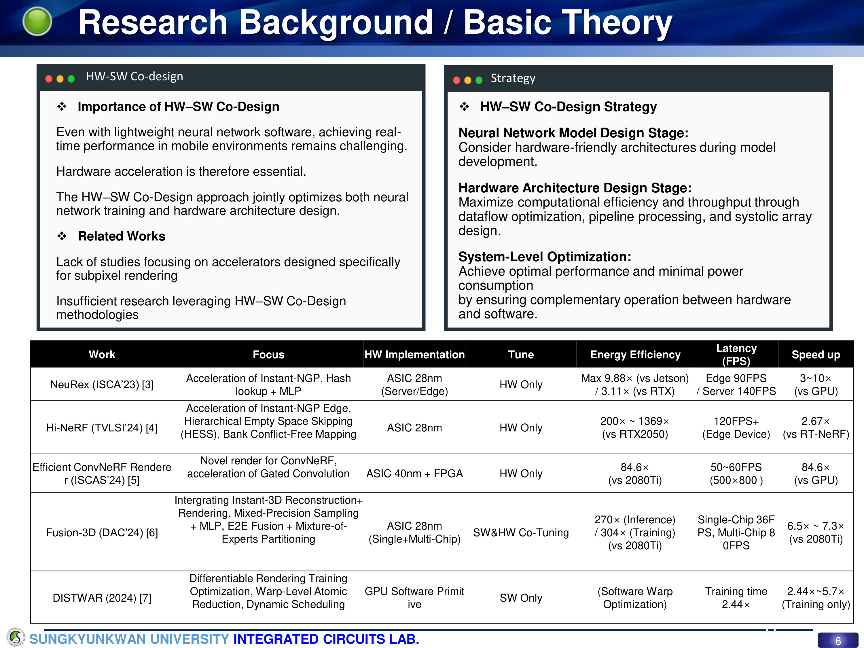
To solve this, we applied a hardware–software co-design strategy that combines model compression and hardware acceleration to meet both performance and power requirements.
Notably, very few previous studies have designed accelerators specialized for subpixel rendering, and even fewer have applied HW–SW co-design methodologies
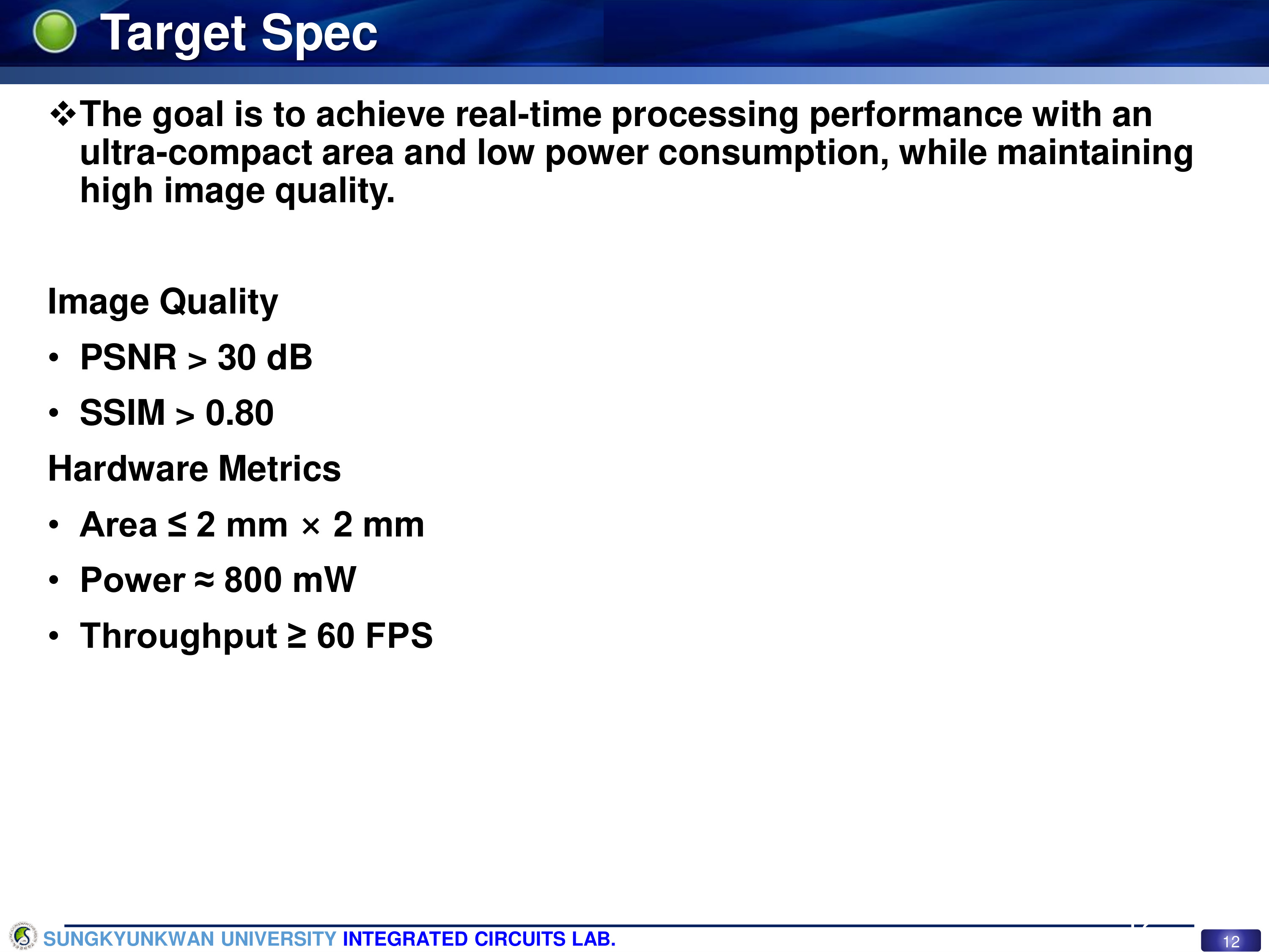
Our final design target is a 45-nm ASIC that achieves:
- PSNR ≥ 30 dB, SSIM ≥ 0.8,
- Chip area ≤ 2 mm × 2 mm,
- Power consumption ≈ 800 mW, and
- Processing speed ≥ 60 FPS.”

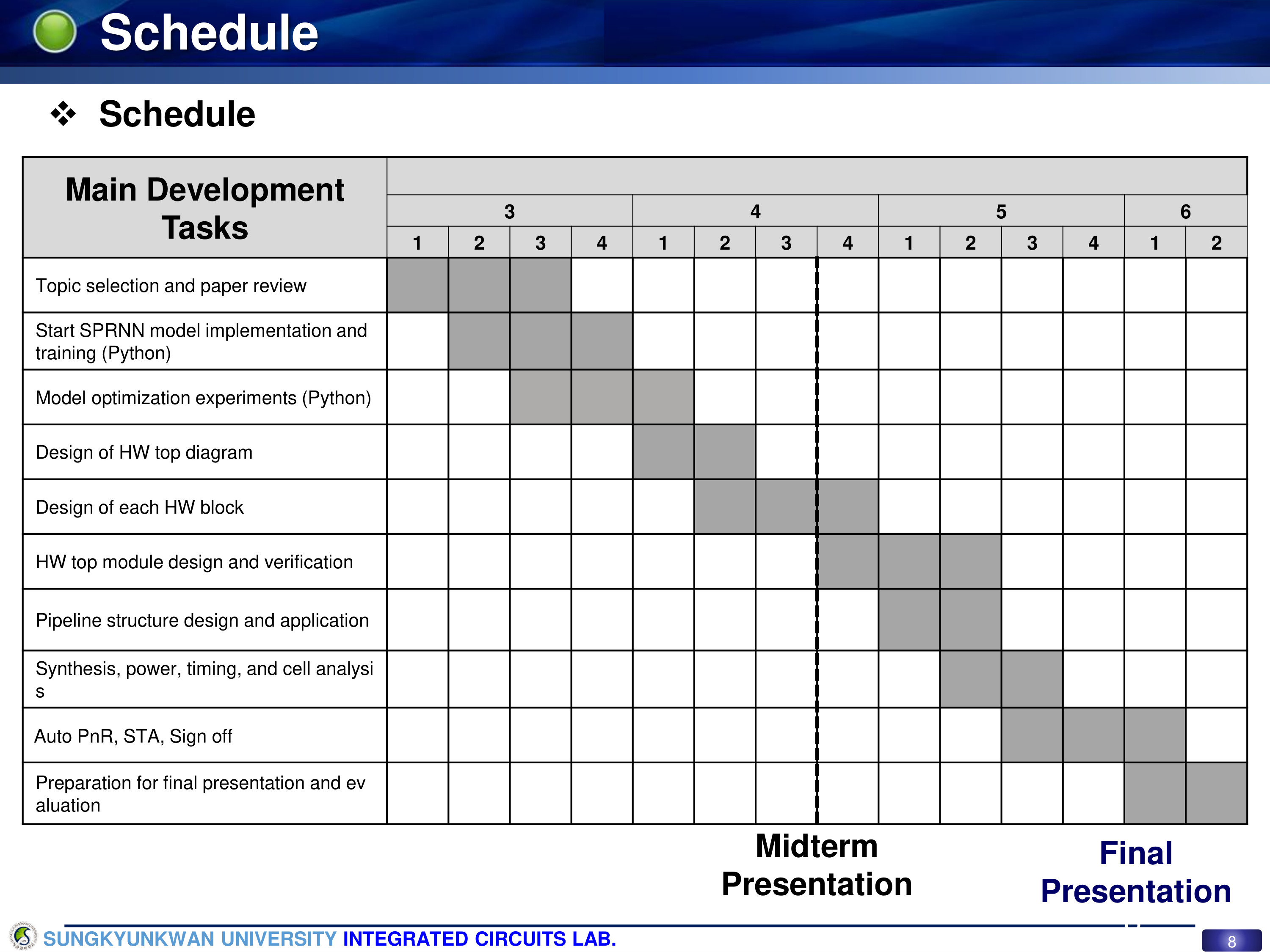
The development schedule is shown here, and all stages were completed according to plan.

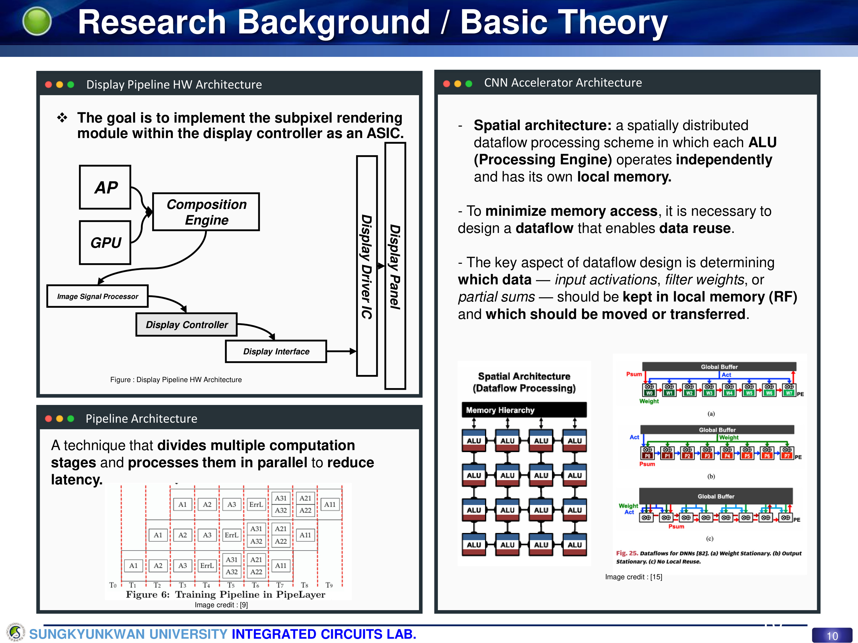
The goal of this work is to implement the Subpixel Rendering module within the Display Controller as an ASIC.
We adopted a spatial architecture that enables spatially parallel dataflow computation.
Additionally, a pipelined processing method was applied by dividing operations into multiple stages to enhance throughput.
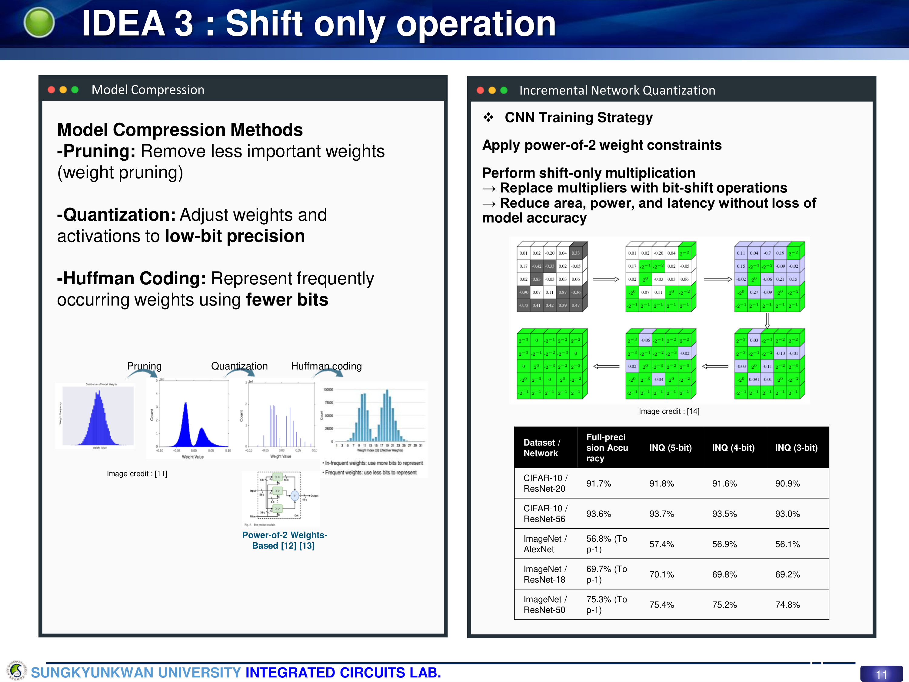
We used Incremental Network Quantization (INQ) during CNN training to constrain weights to powers of two.
This allows multiplication operations to be replaced entirely by bit-shift operations significantly simplifying hardware.
INQ progressively quantizes the most critical weights to power-of-two values while continuing to fine-tune the remaining parameters, thus maintaining accuracy.

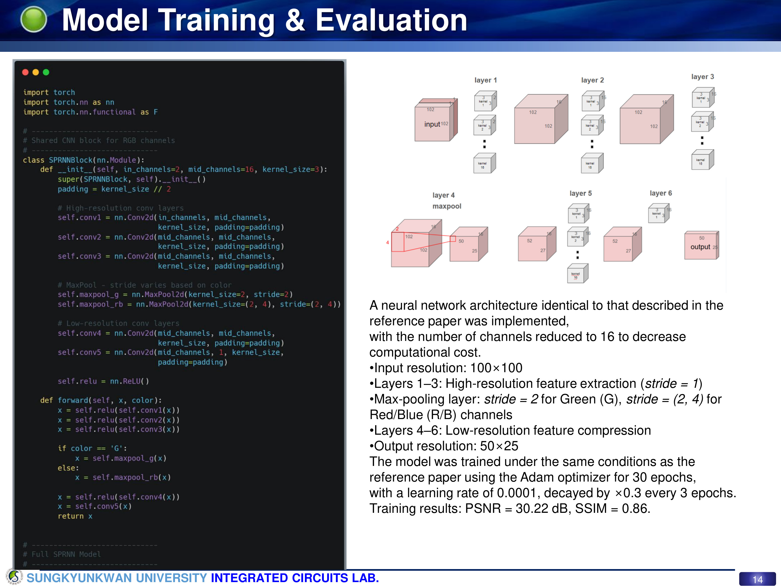
We implemented the CNN model identical to that in the reference paper using PyTorch.
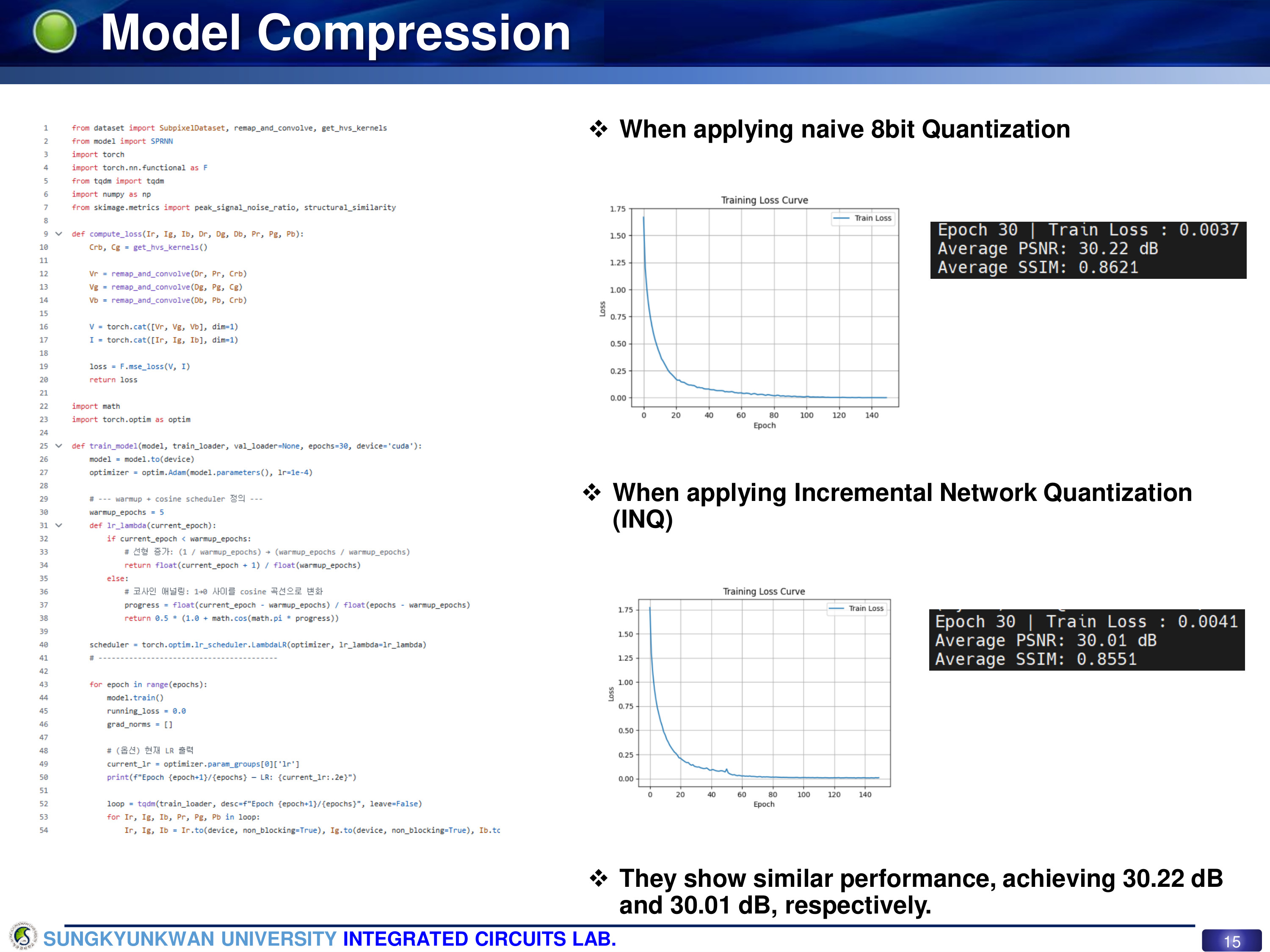
The training achieved PSNR = 30.22 dB and SSIM = 0.86, meeting our target performance.
Next, we applied INQ-based model compression.
After retraining with power-of-two weights, the model achieved 30.01 dB PSNR, showing minimal degradation compared to the original model.
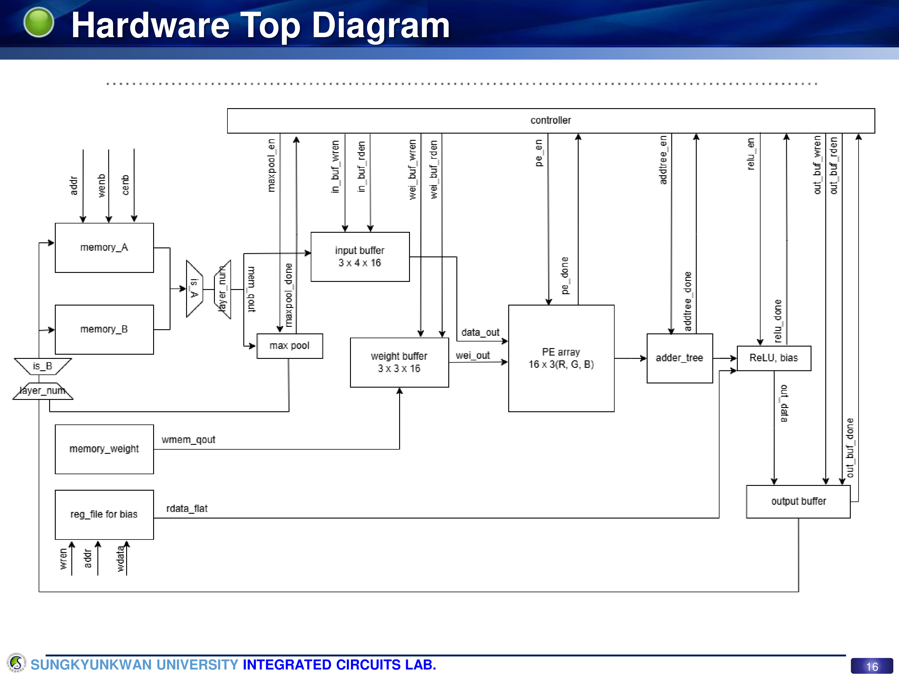
The top-level hardware diagram consists of computation modules, buffers, memory blocks, and a controller, as shown in the figure
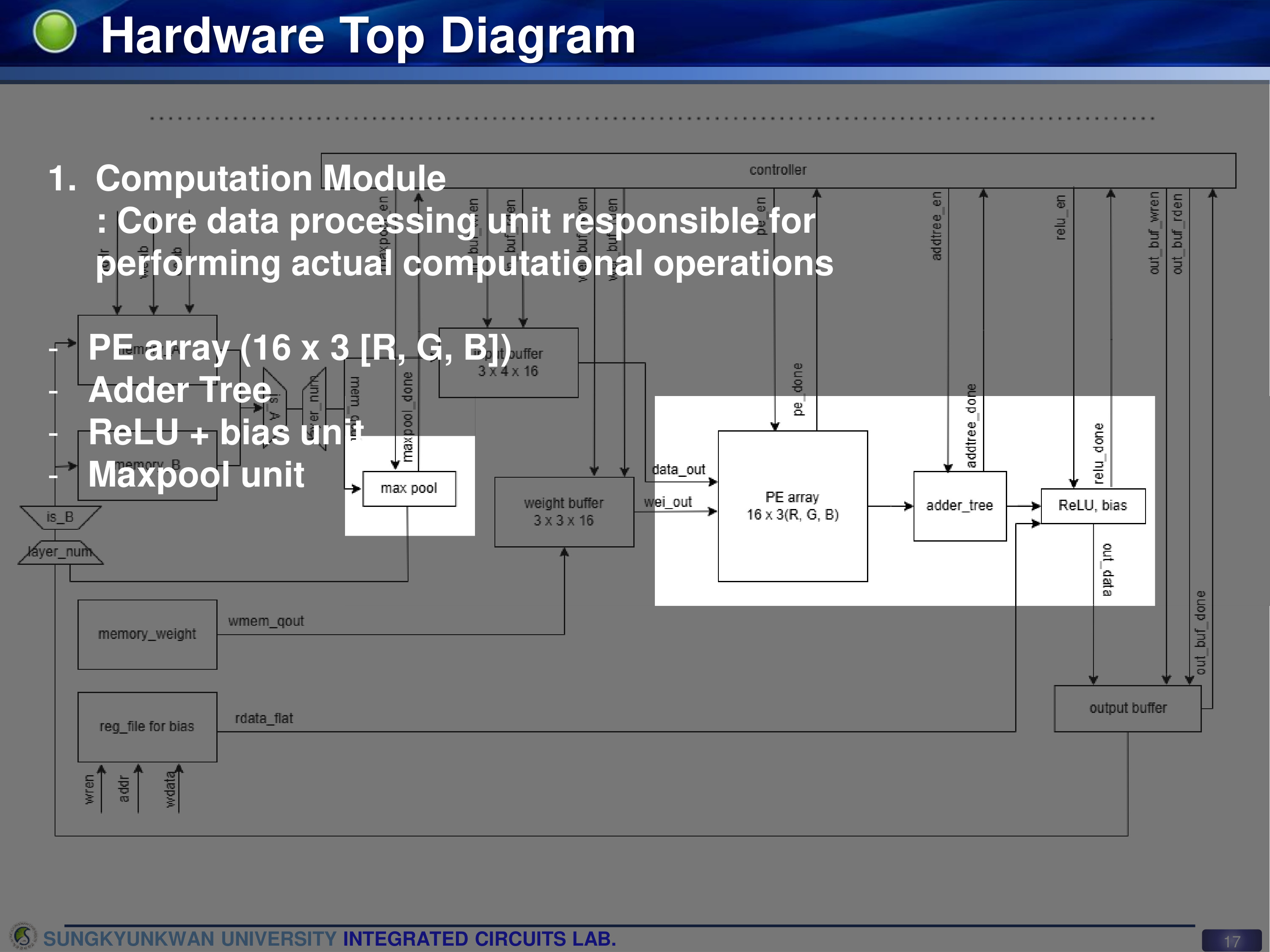
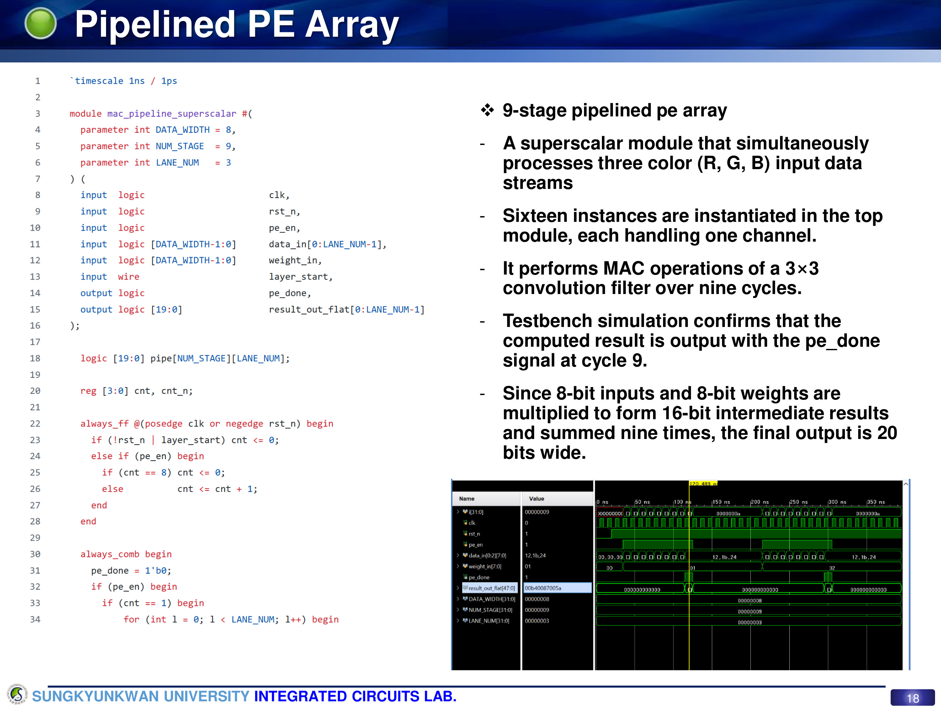
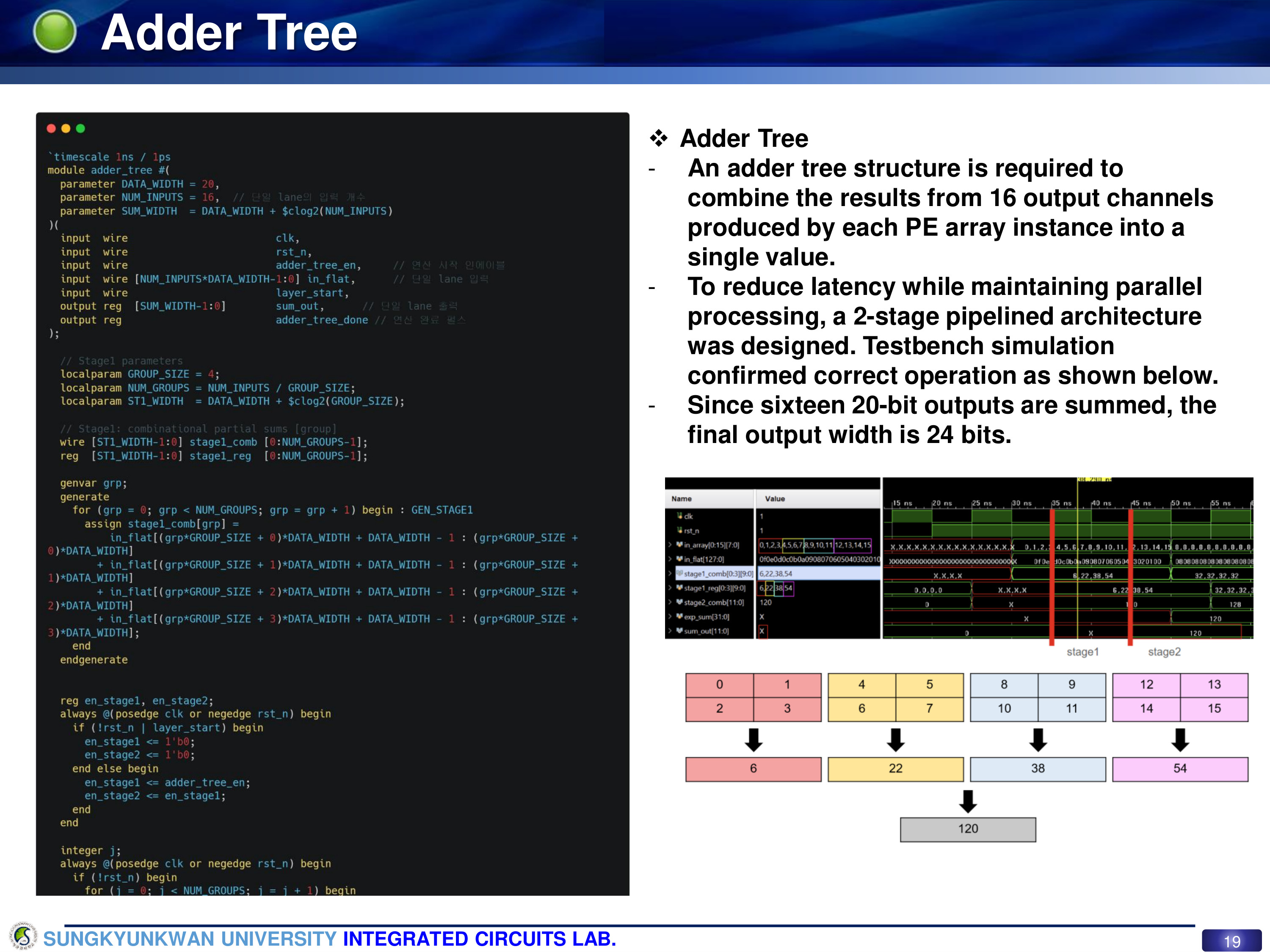
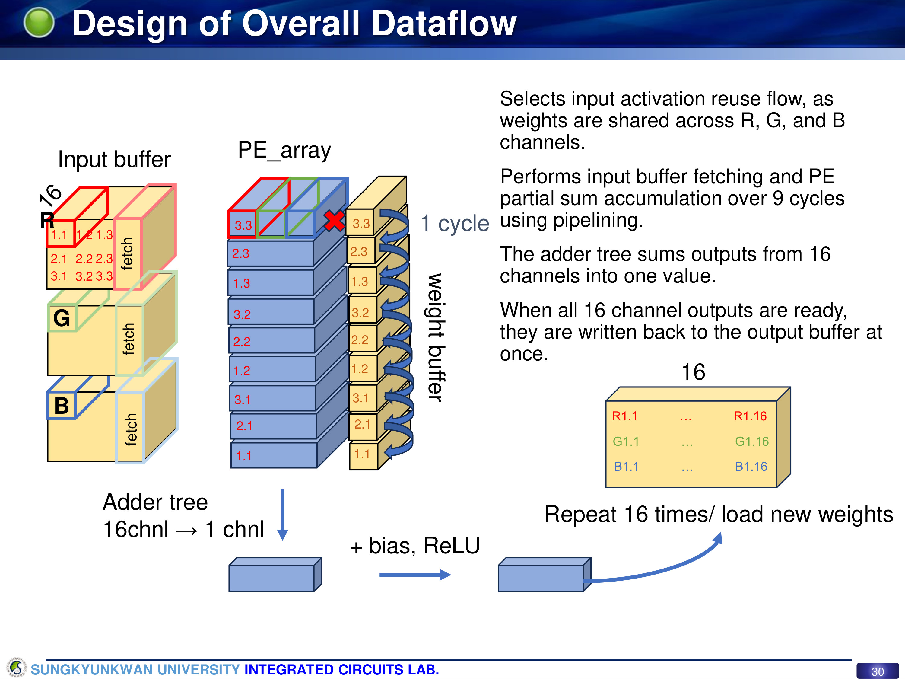
The pipelined PE array consists of 16 superscalar PEs, each performing a 3×3 MAC operation for RGB channels over 9 cycles, producing 20-bit outputs. Both design and simulation were completed. A two-stage adder tree was designed and simulated to sum the partial results from 16 channels
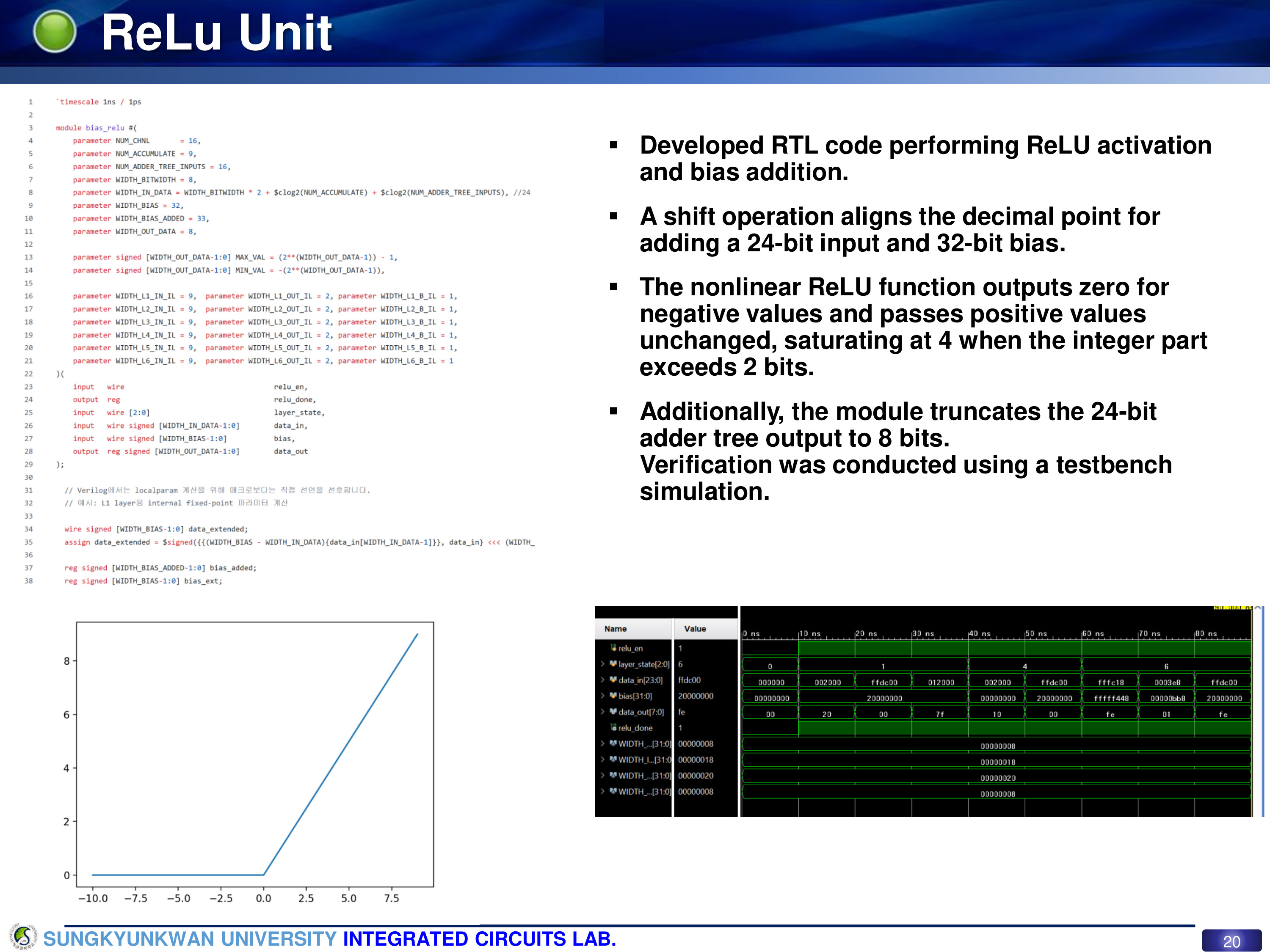
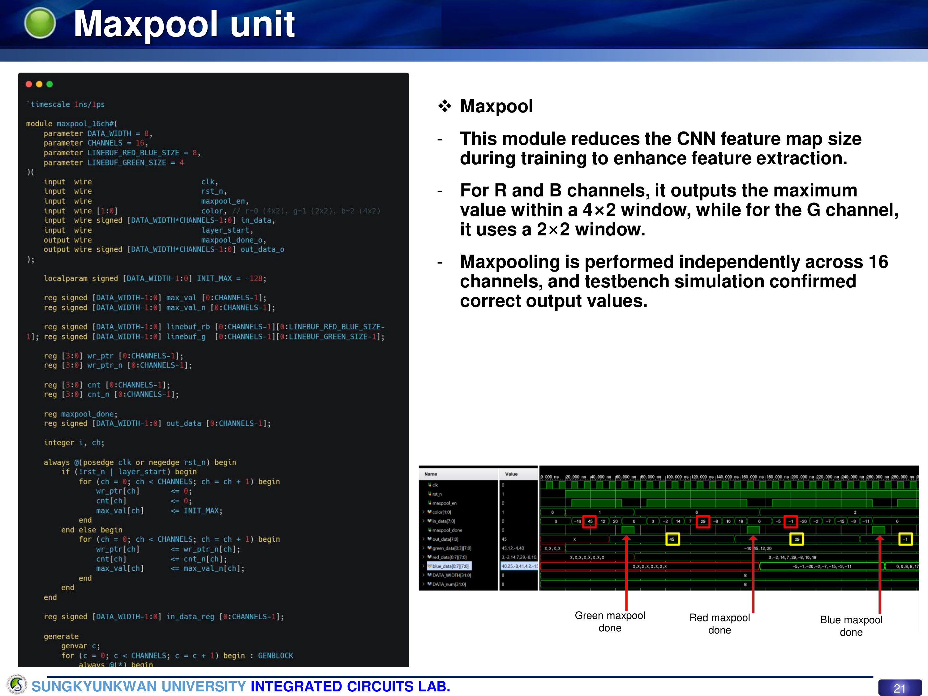
The ReLU–bias module aligns a 24-bit input with a 32-bit bias via shift operations, performs bias addition, applies the ReLU activation, and truncates the result to 8 bits. The module was fully implemented and verified. We also designed and verified the Maxpool unit, which performs max-pooling operations.
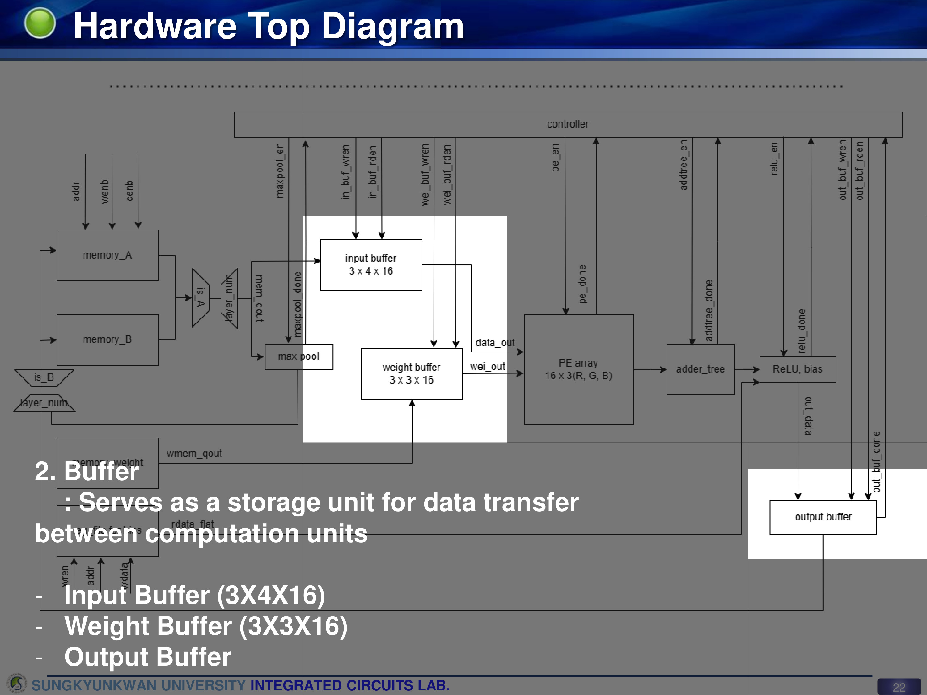
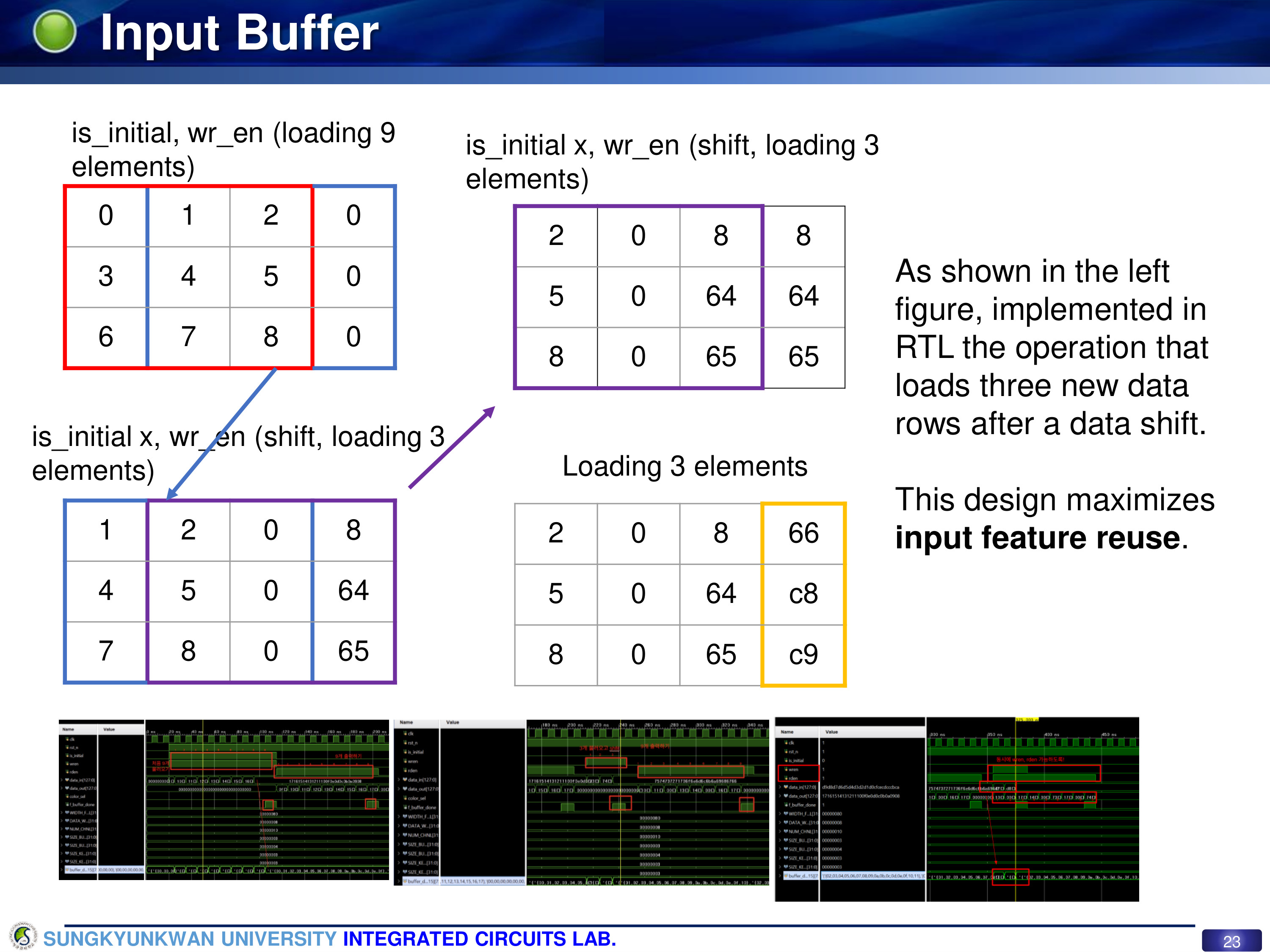
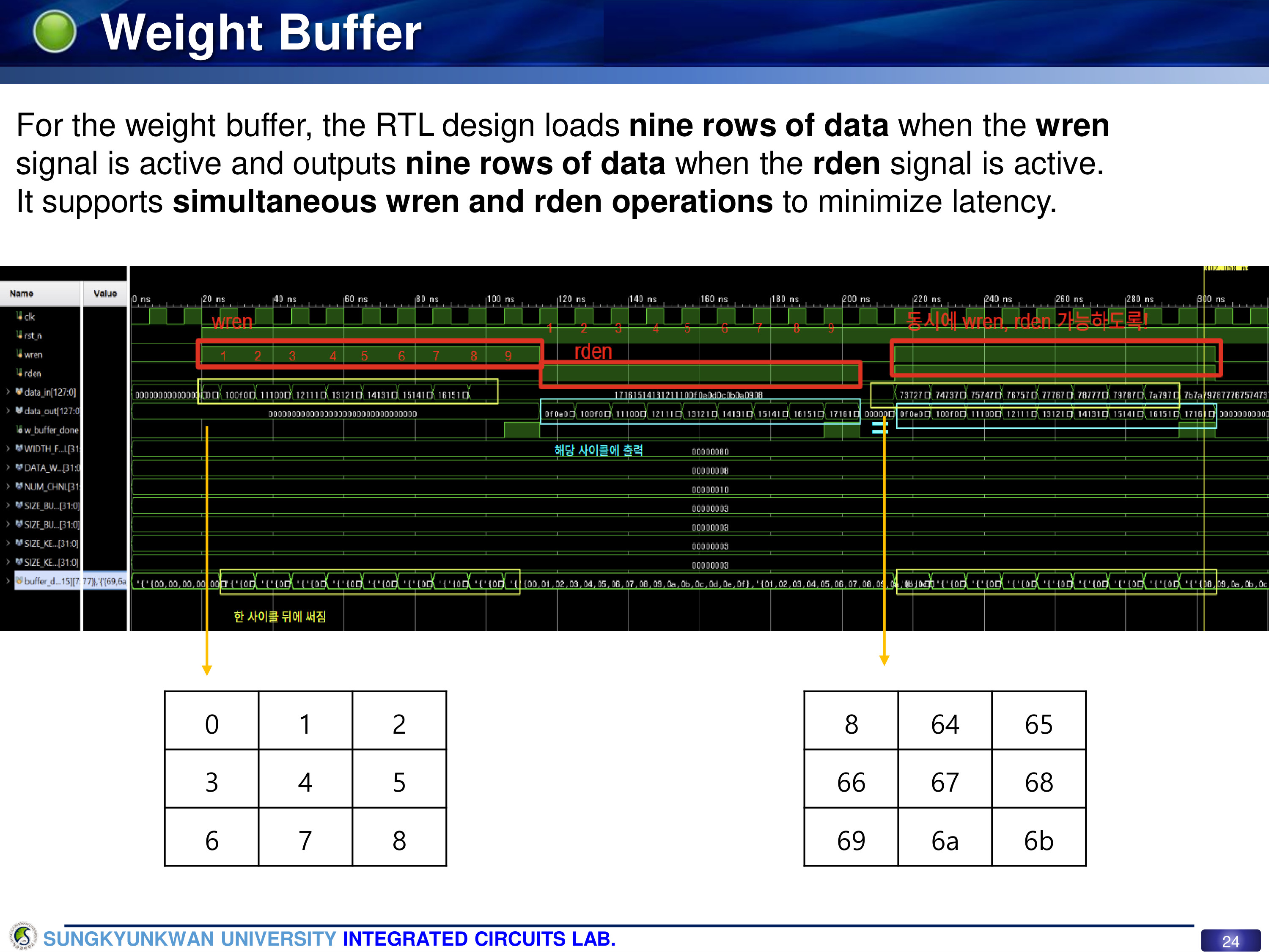
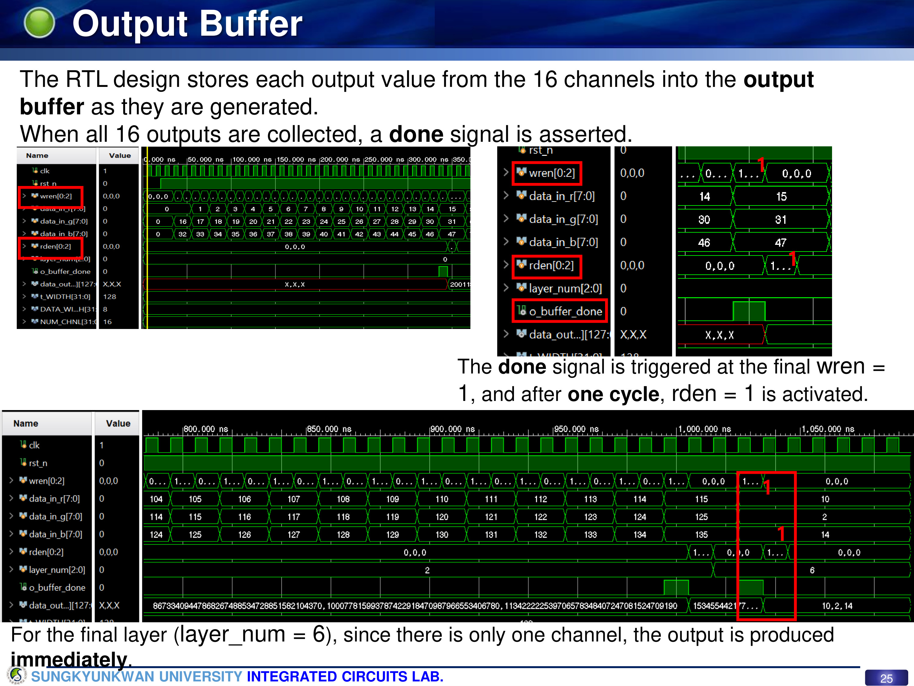
The buffer temporarily stores and outputs data fetched from SRAM. The input buffer was designed to perform data-shift operations to maximize data reuse. The weight buffer supports simultaneous read and write operations, minimizing latency. The output buffer stores each channel output and performs a single write-back to SRAM once all 16 channel results are ready.
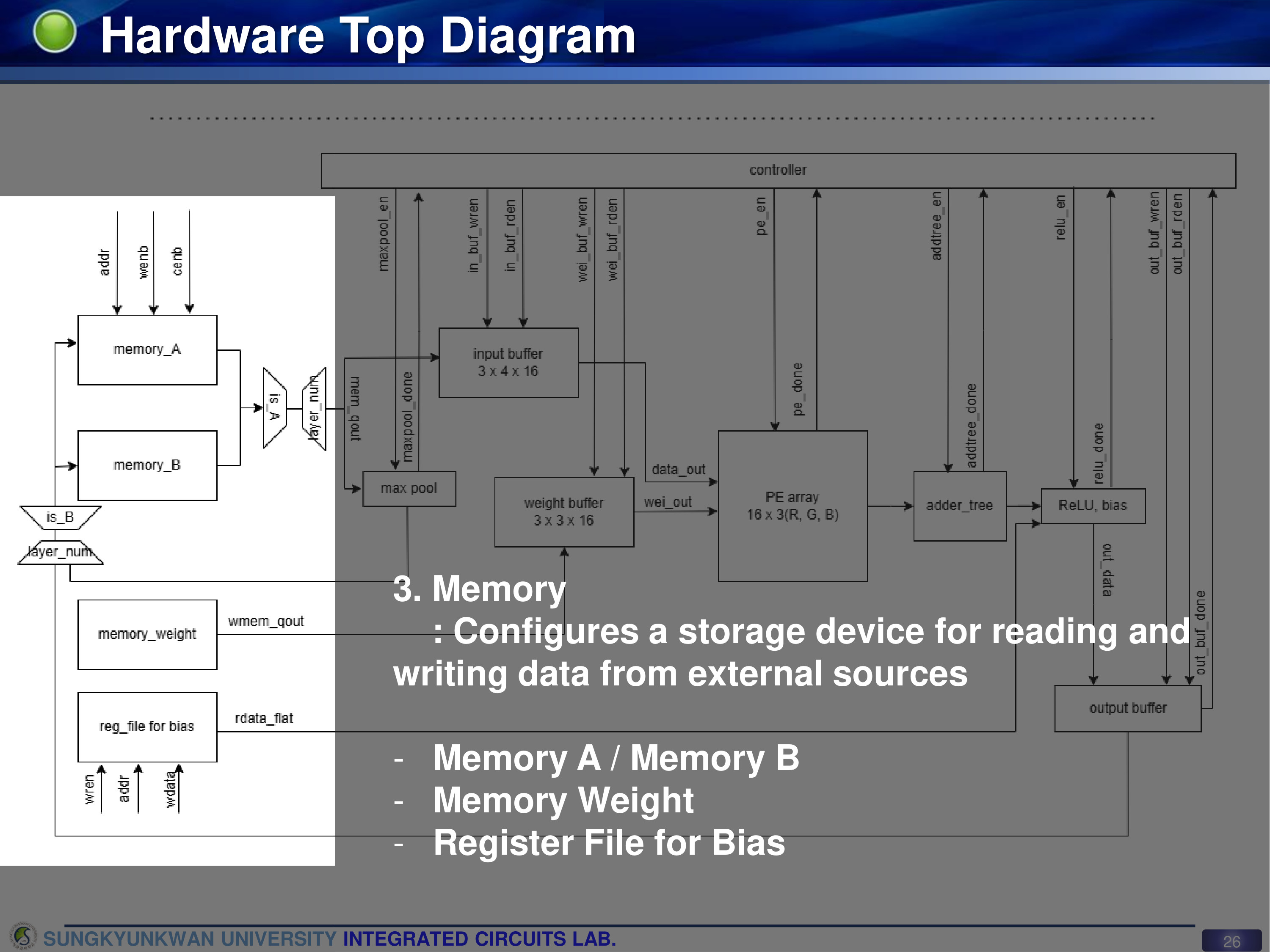
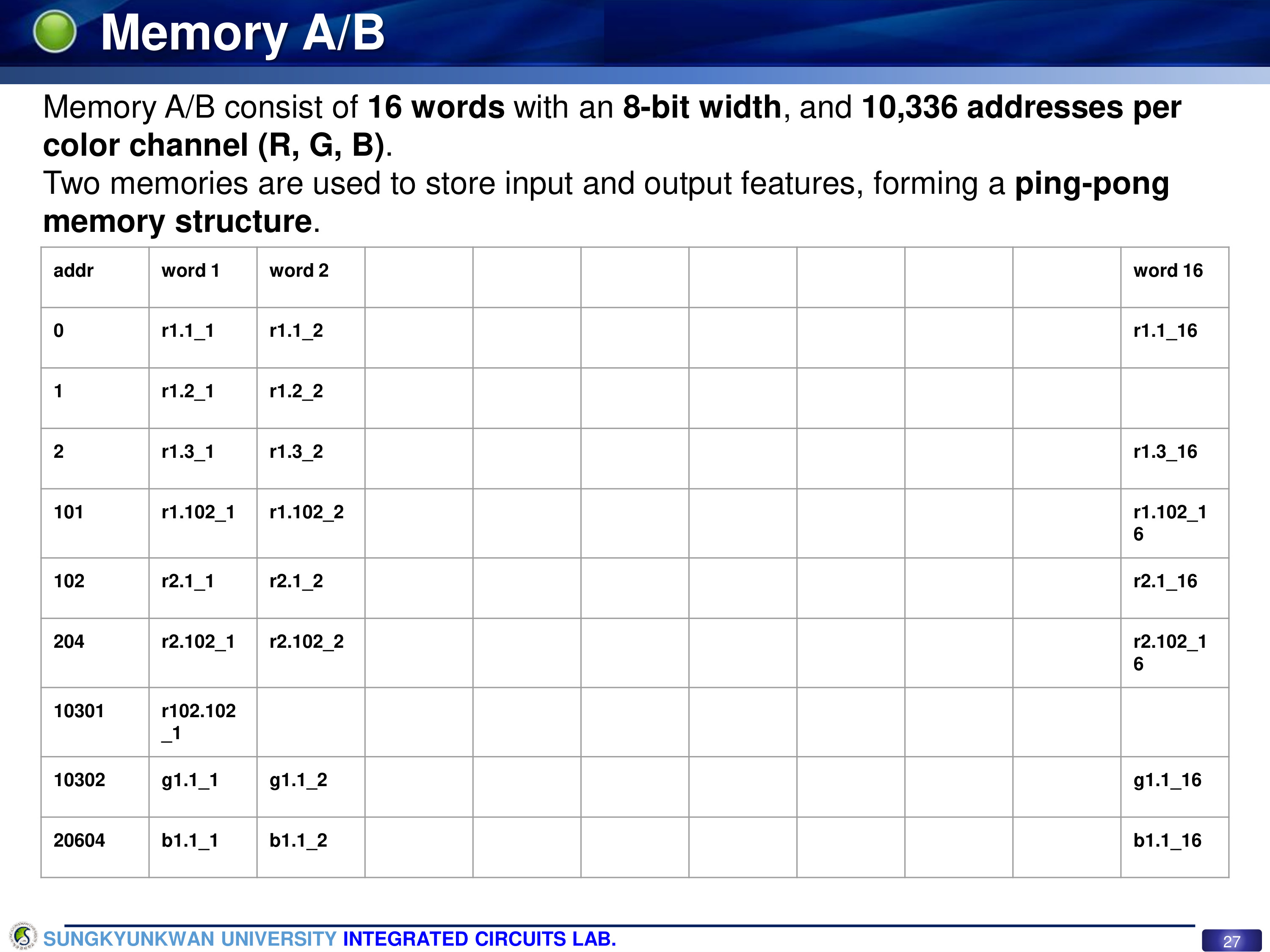
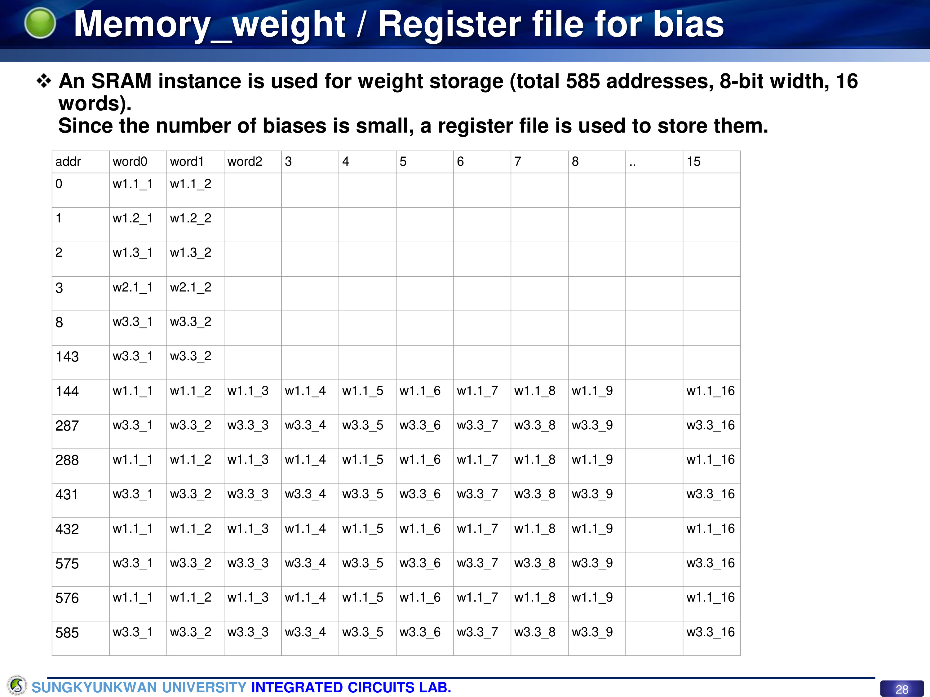
The memory stores the input feature maps, weights, and biases. The input feature memory is divided into two banks, A and B, forming a ping-pong structure that alternately stores feature maps between layers. The weight memory and bias register file store and output the respective parameters.
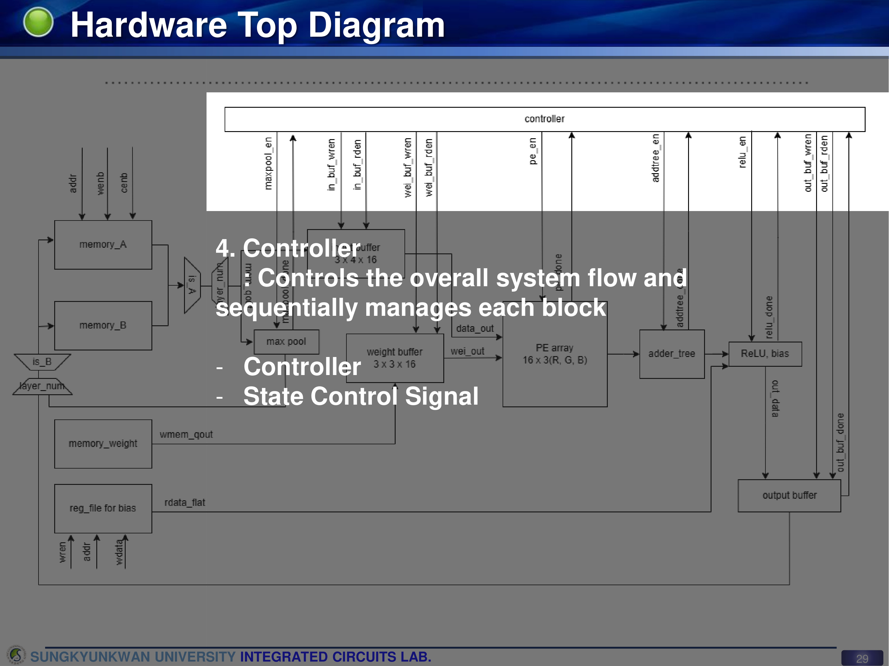
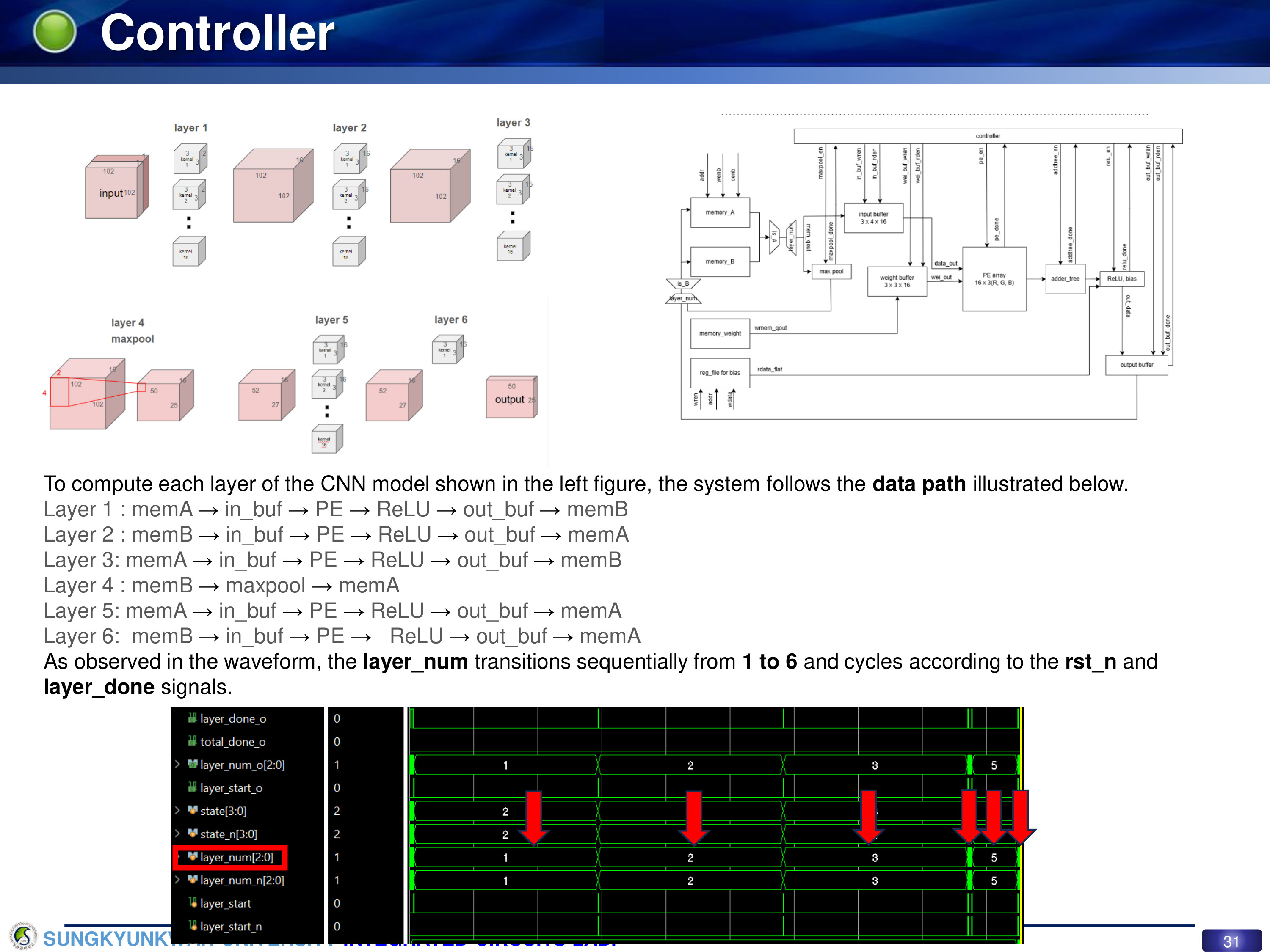
The top controller manages the entire system operation.
As shown in the dataflow diagram, each module is orchestrated so that input features are fetched into buffers while PEs concurrently perform 3×3 convolution over a 9-cycle pipeline, minimizing overall latency.
The left figure shows the CNN model computation mapped onto the right hardware architecture, illustrating the overall processing flow.
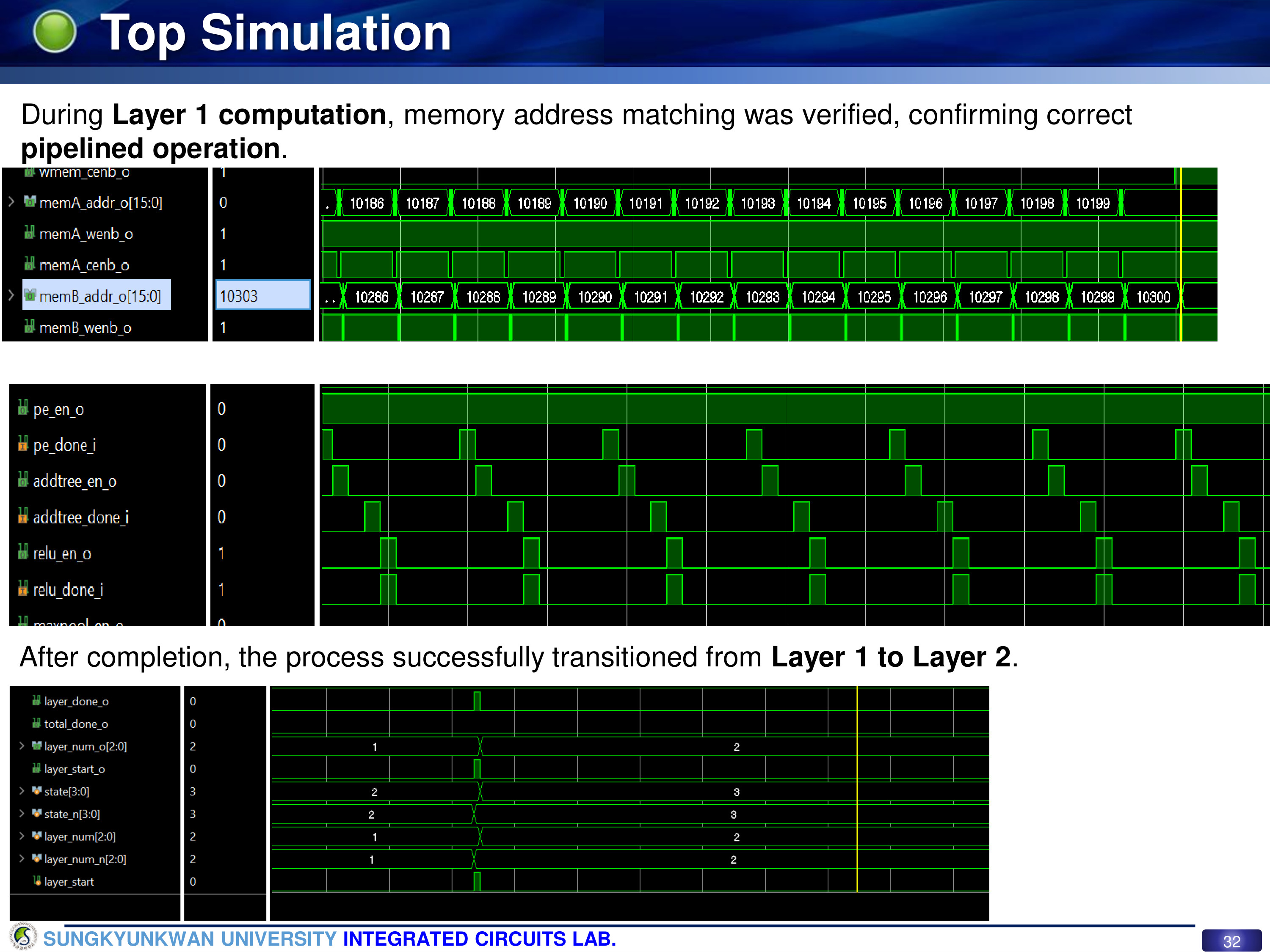
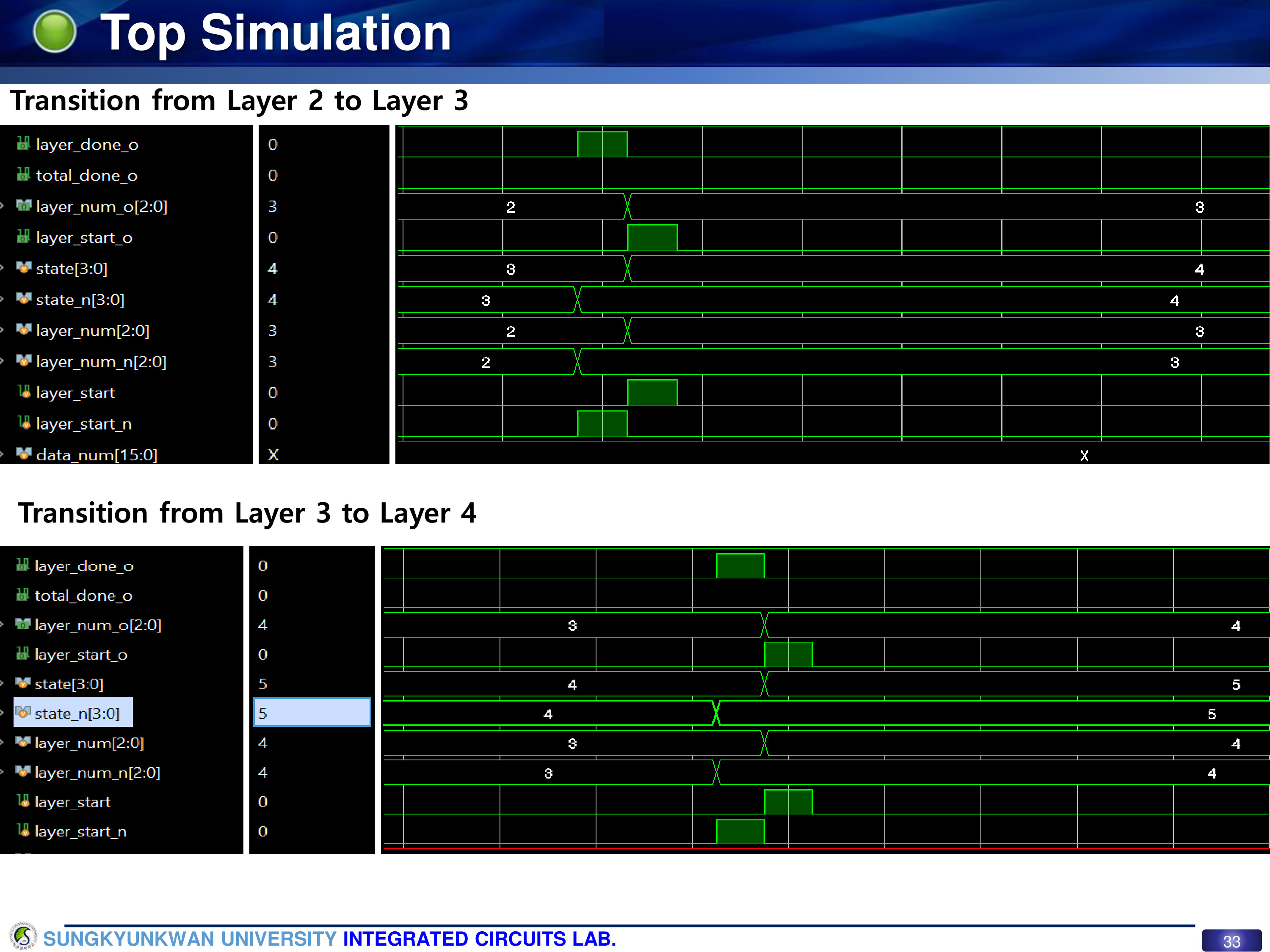
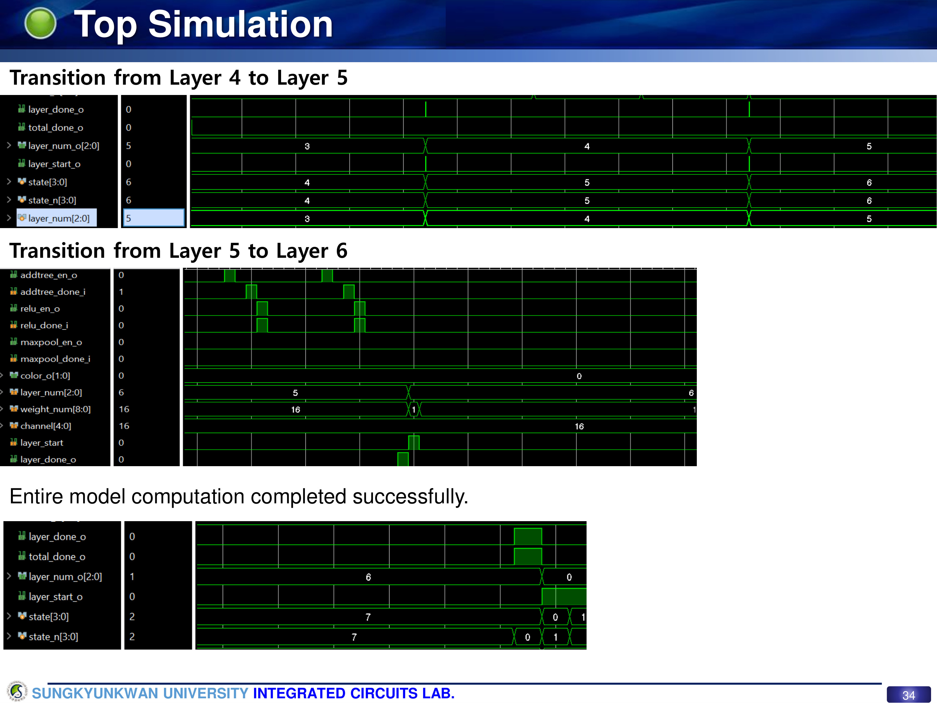
The top-level simulation confirmed correct memory address mapping and pipeline operation, as well as proper data transfer between layers.
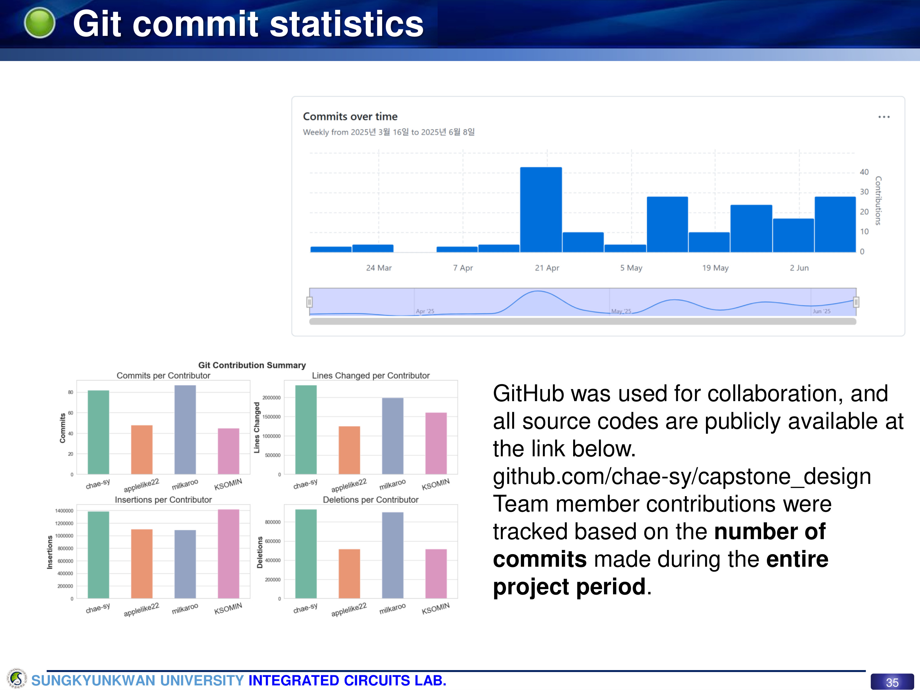
Project management was conducted via GitHub, with a total of approximately 300 commits recorded.
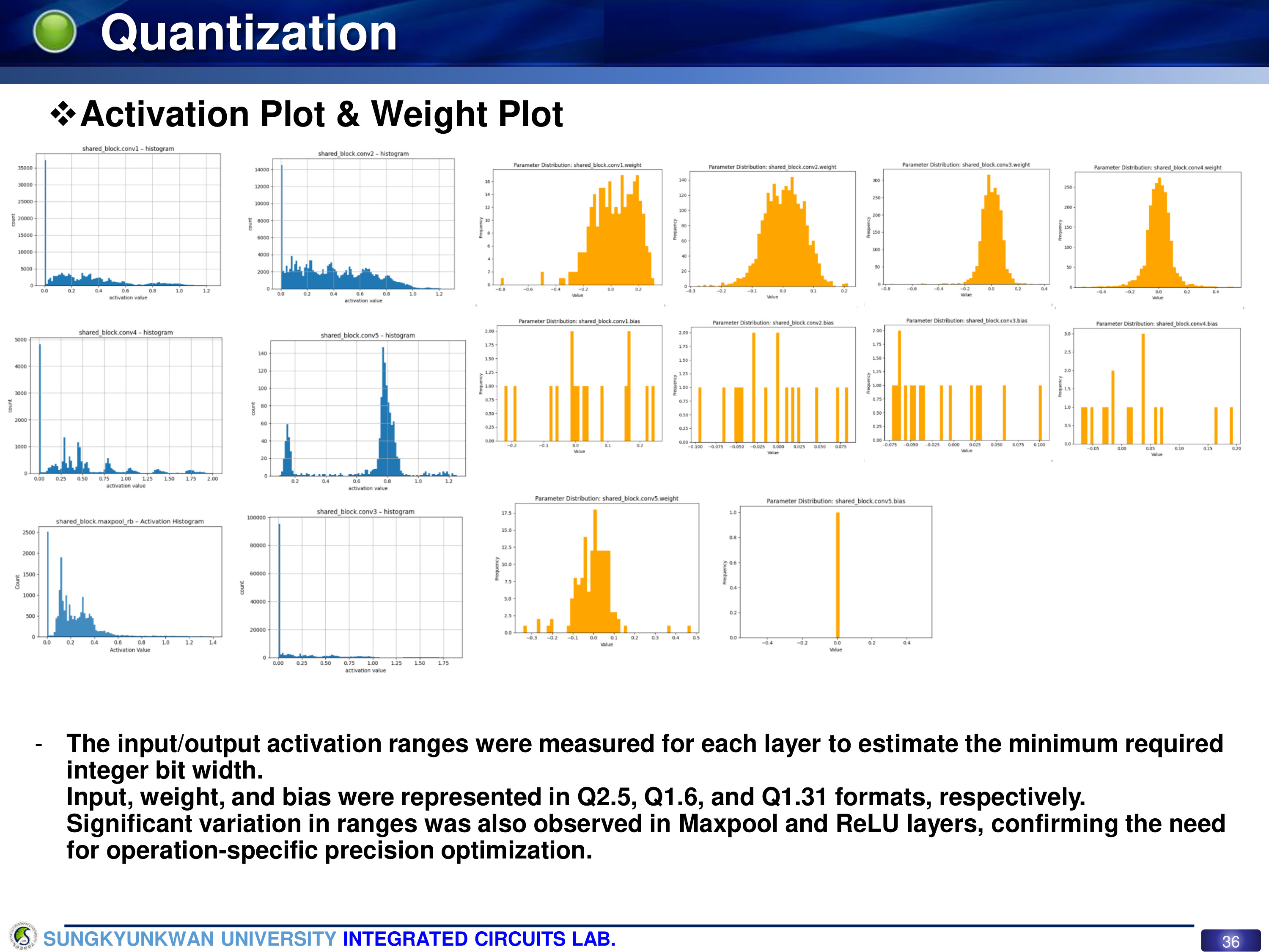
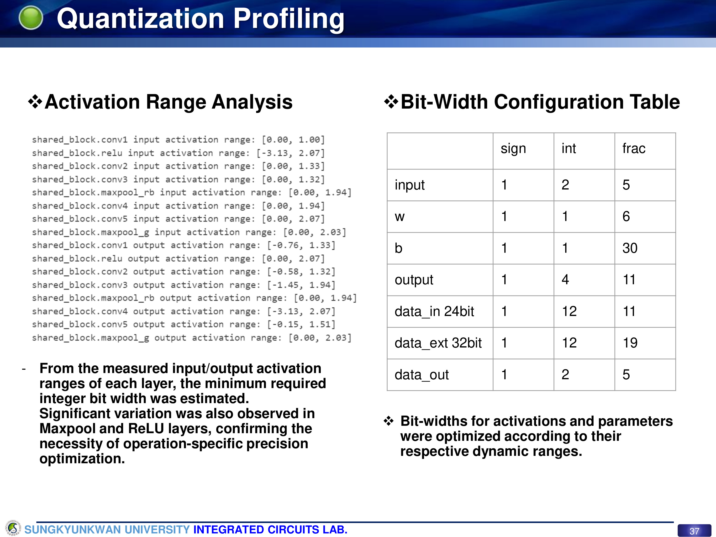
Through quantization profiling, we analyzed the integer and fractional bit requirements for each operation.
We selected Input = int2 + frac5, Weight = int1 + frac6, and Bias = int1 + frac31 configurations. The final bit-width configuration is summarized in the table.
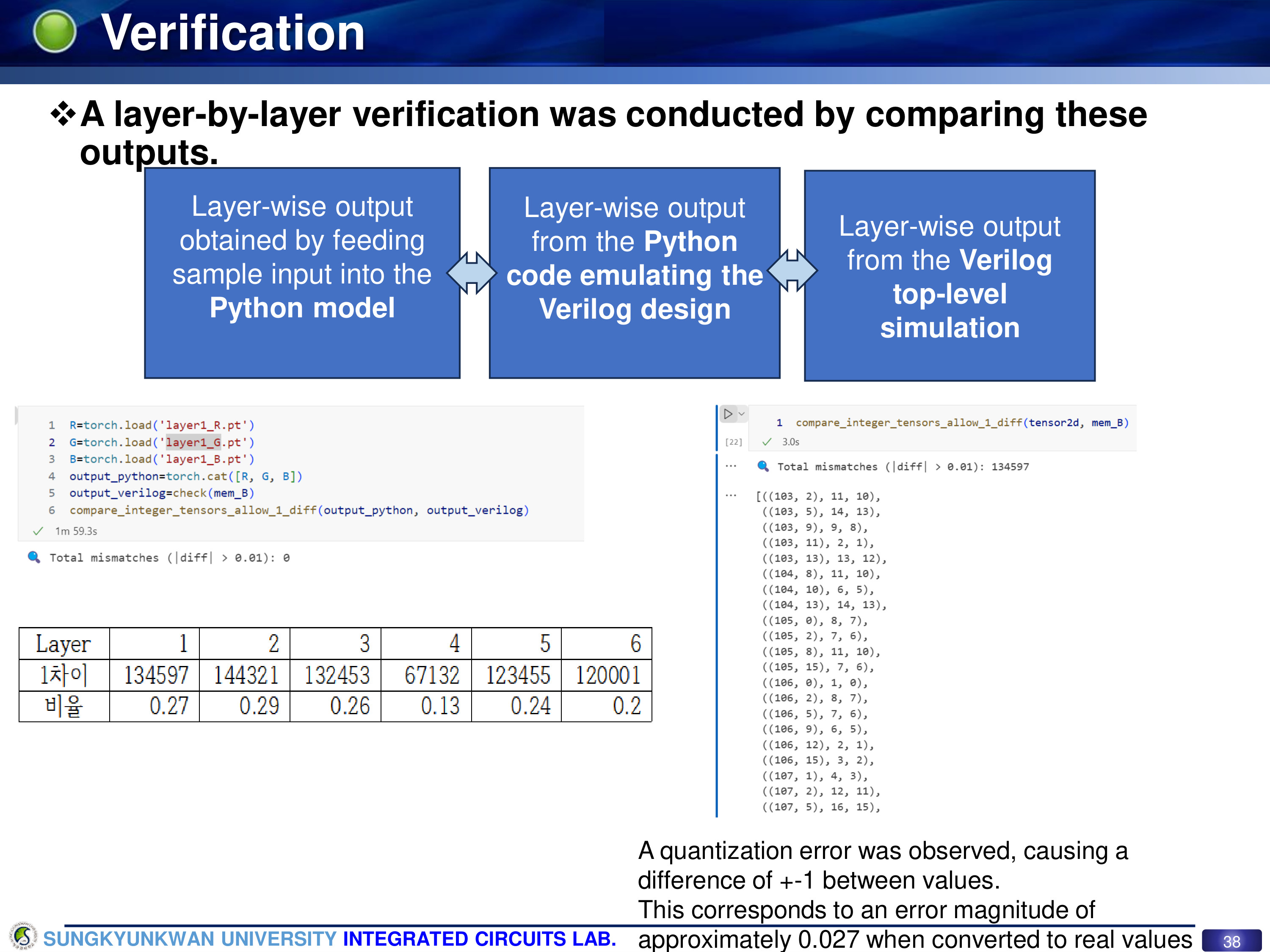
In the verification stage, layer-wise output comparisons confirmed that the quantization error was within ±1 LSB, corresponding to 0.027 in real value.
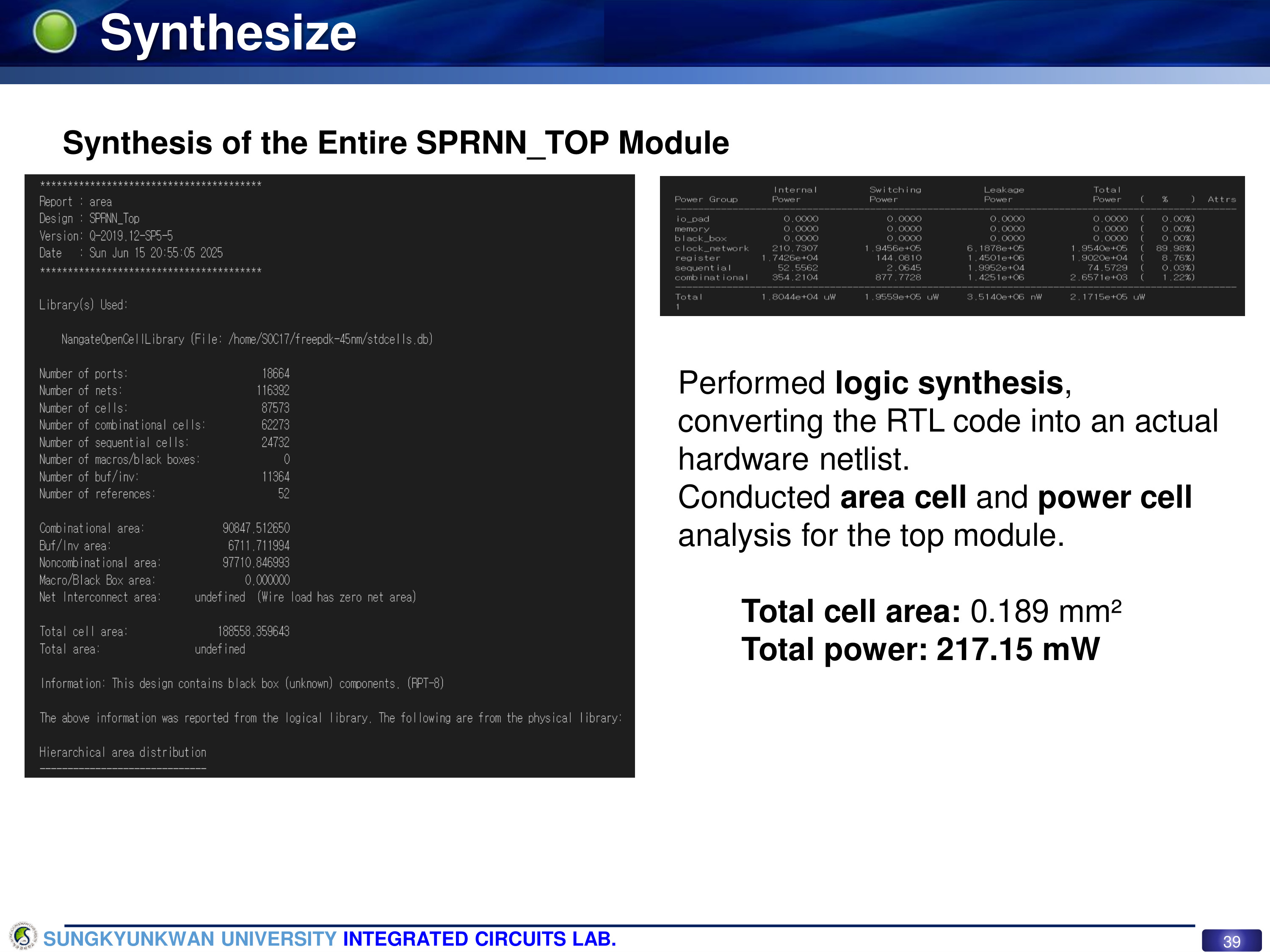
The synthesis result of the full SPRNN_TOP module showed a cell area of 0.189 mm² and total power consumption of 217 mW.
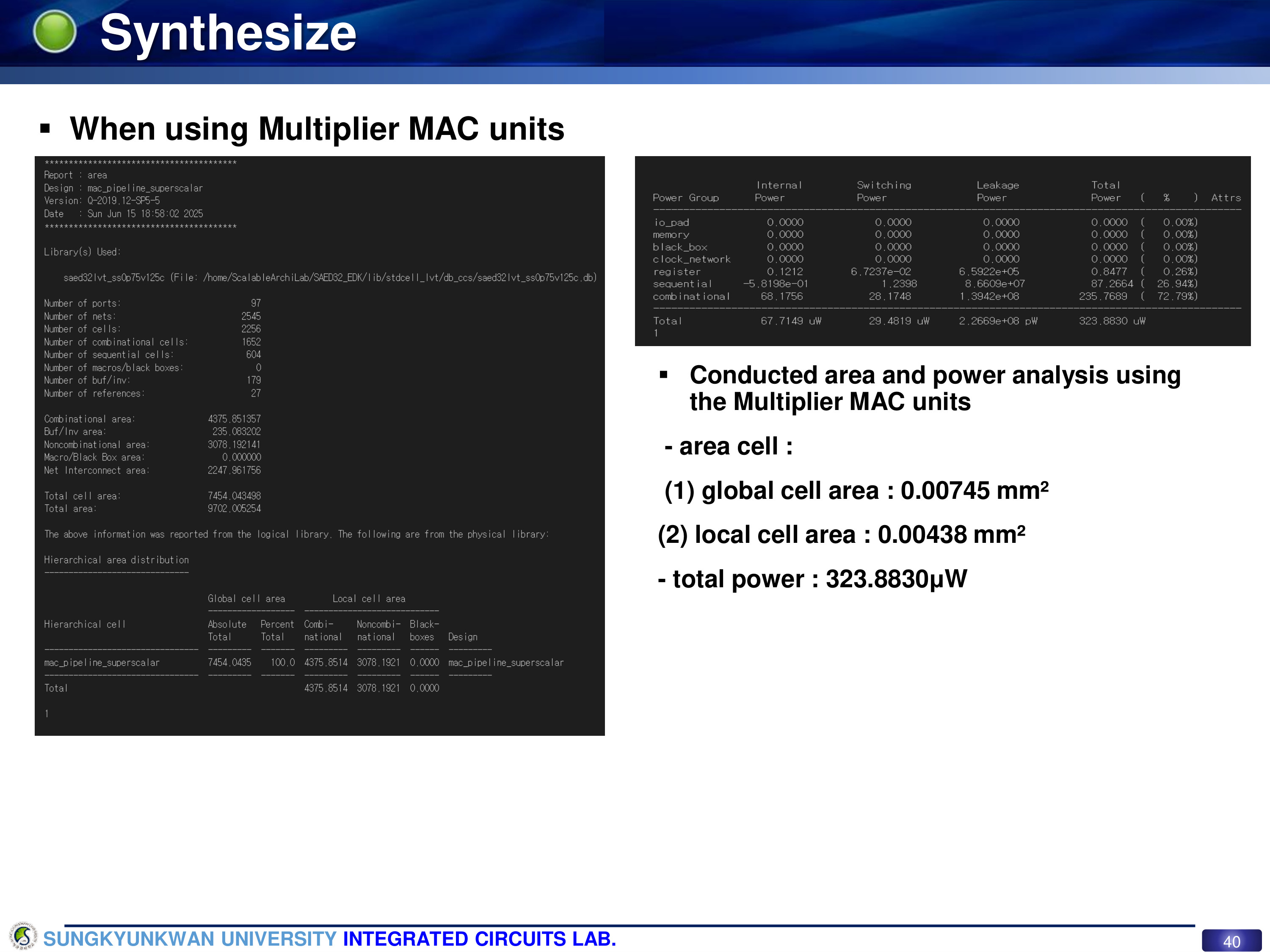
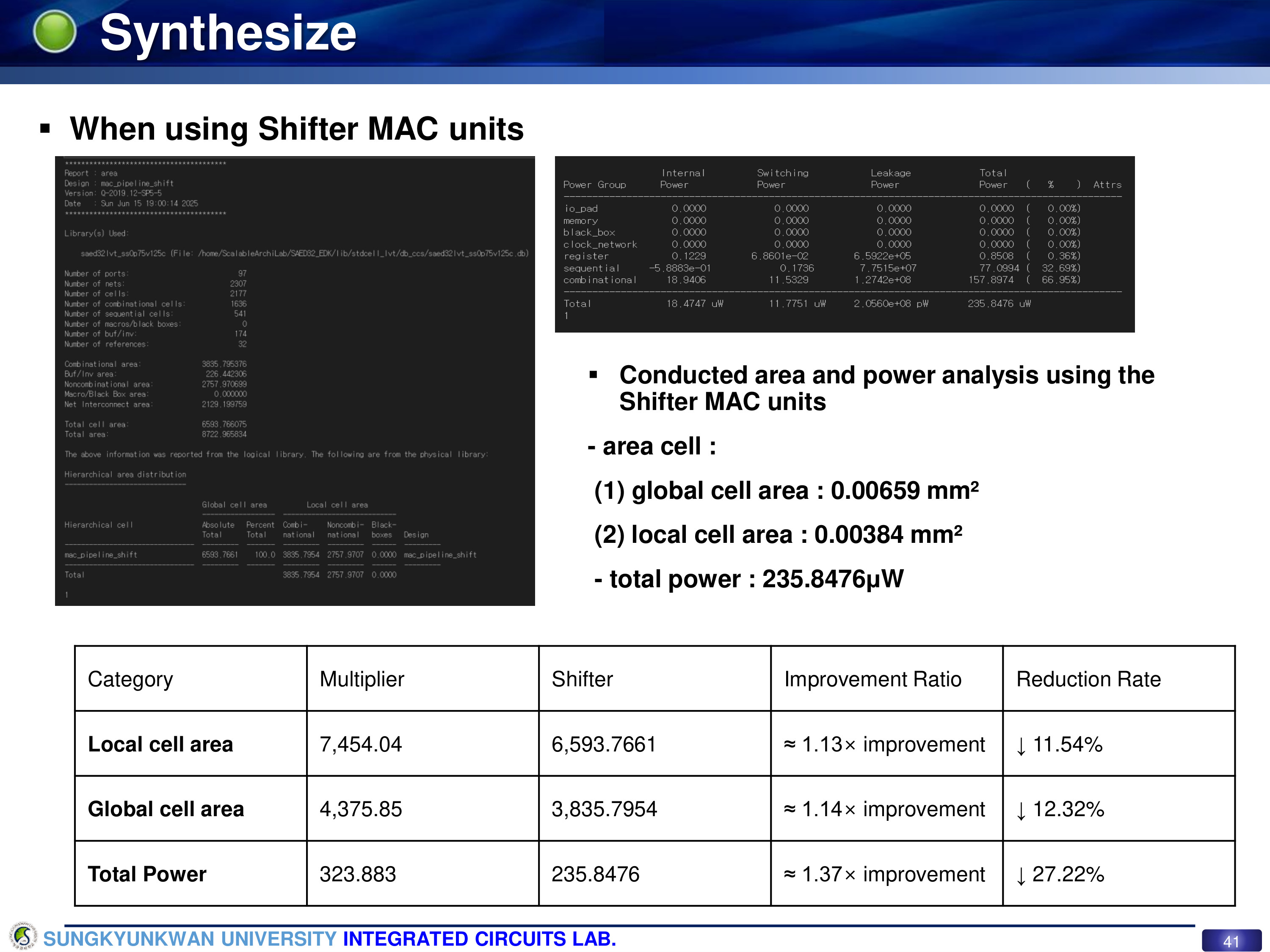
Comparing PE arrays implemented with multipliers versus shifters, synthesis results demonstrated an 11% area reduction and 27% power savings.
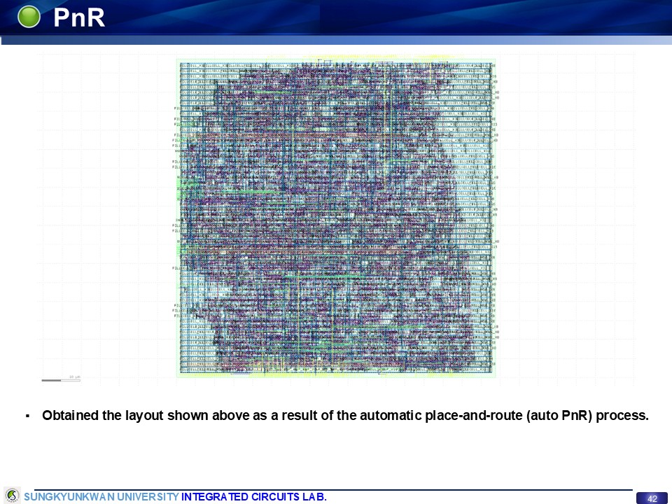
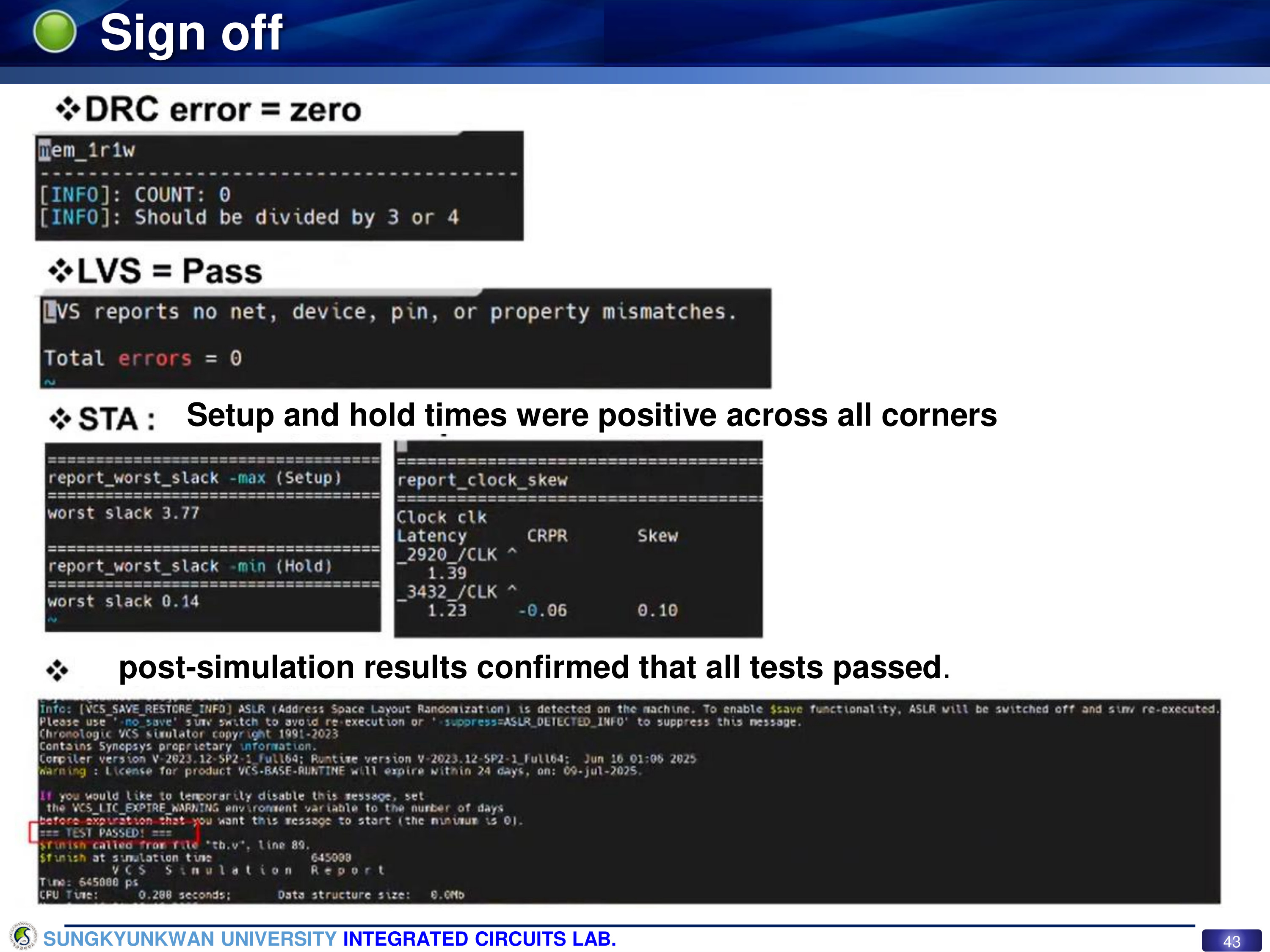
Using OpenLane, we performed automatic place-and-route (auto PnR). The layout achieved DRC zero, LVS pass, and positive setup/hold margins across all corners. (Post-layout simulation, though not included in the slides, was also confirmed as TEST PASSED.)

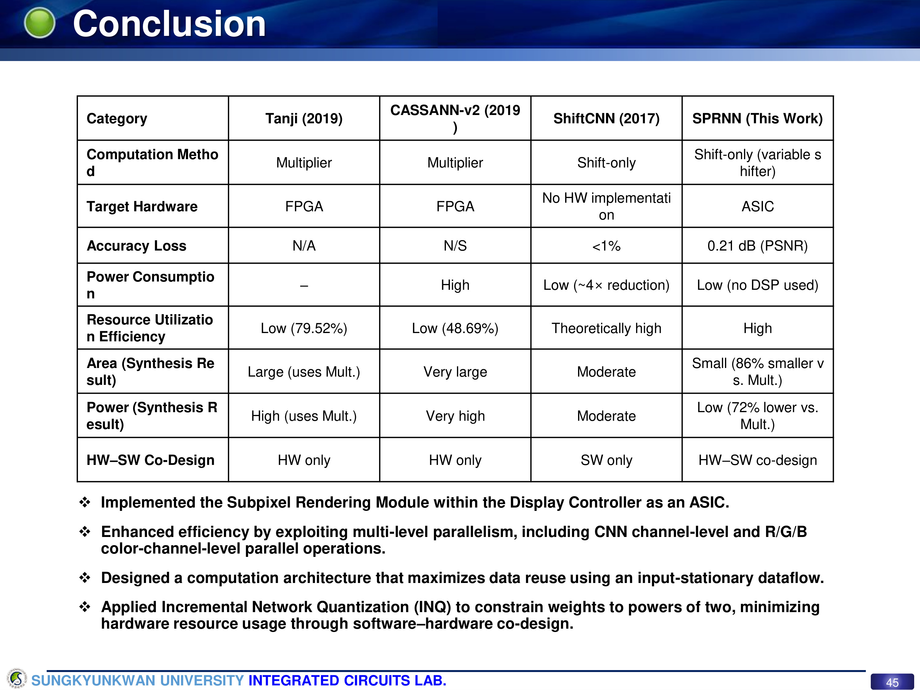
Finally, we will present our conclusion.
- Implemented a CNN-based Subpixel Rendering module as an ASIC.
- Maximized efficiency through multi-level parallelism and input-stationary dataflow.
- Achieved substantial area and power reductions via INQ-based shift-only computation.
The key contribution of our work lies in achieving target specifications through a hardware–software co-design approach, surpassing prior research.